ASML has become the overlord in the field of lithography machines and will move towards 2nm and 3nm processes.
Text: Shi Yaqiong, Li Yajing
Editor: Shi Yaqiong
**
With China’s chip security issues, lithography machines have also become the focus of the industry.
It is priced at over 100 million U.S. dollars and is still in short supply. It is considered to be an important promoter of Moore’s Law at the moment, and is better than the “money printing machine” of chip companies. It is a collection of various disciplines. The equipment weighs dozens of tons and requires multiple Boeing aircraft to transport. It is considered the crown jewel of the semiconductor industry. Although it is an industrial equipment and commercial product, its destiny has never escaped the competition and cooperation game between big countries.
At the moment when Moore’s Law is challenging the physical limit of 2nm, superimposed on complex international relations, lithography machines have become one of the industries that should be understood in 2020. For this reason, we have done this light industry research, hoping to truly present the past, present and future of this industry.
We hope to answer the following questions in this article:
Why is the lithography machine so important to the chip industry?
Why is the most advanced lithography machine so difficult to develop?
What is the current global lithography machine industry pattern? How did ASML become the most important lithography player?
Where is the gap between domestic lithography machines and foreign countries?
Why is there such a gap between Chinese and foreign lithography opportunities?
As the lithography machine approaches the limits of physics, materials science, and precision manufacturing, what development trend will it present in the future?
1. Why is the lithography machine so important-“If we can’t hand over the EUV lithography machine, Moore’s Law will stop here”
How important is the lithography machine?
As the most cutting-edge company in the world’s lithography machine, the Dutch ASML company said-“If we can’t hand over the EUV lithography machine, Moore’s Law will stop there.”
For more than 50 years, the semiconductor industry has been following the economic law of Moore’s Law: The number of components that can be accommodated on an integrated circuit every 18 months Will double. This means that every 18 months, in order to achieve more than double the performance of the chip, The chip manufacturing process will be at least doubled.
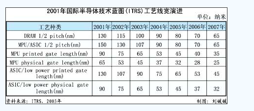
In the early 20th century, the chip nanomanufacturing schedule, the picture comes from the Internet
At the beginning of the 21st century, chips have just entered the hundred-nanometer process. At that time, the threshold of the lithography machine was not high. In 2007, China’s Shanghai Microelectronics Equipment Co., Ltd. was established for five years and developed a 90nm lithography machine that year. In fact, in the early 1970s and 1980s, optical manufacturers such as Nikon and Canon, and chip manufacturers such as Intel made lithography machines.
Nano process forecasting
(1) Why is the lithography machine so important to the chip industry? We can simply disassemble it first.
1. The manufacturing process of the chip
In order to more clearly express the importance of the lithography machine to the chip industry and Moore’s Law, we can first briefly describe the production process of the chip.
You can look at a simple and direct schematic diagram of how the chip is developed and produced:
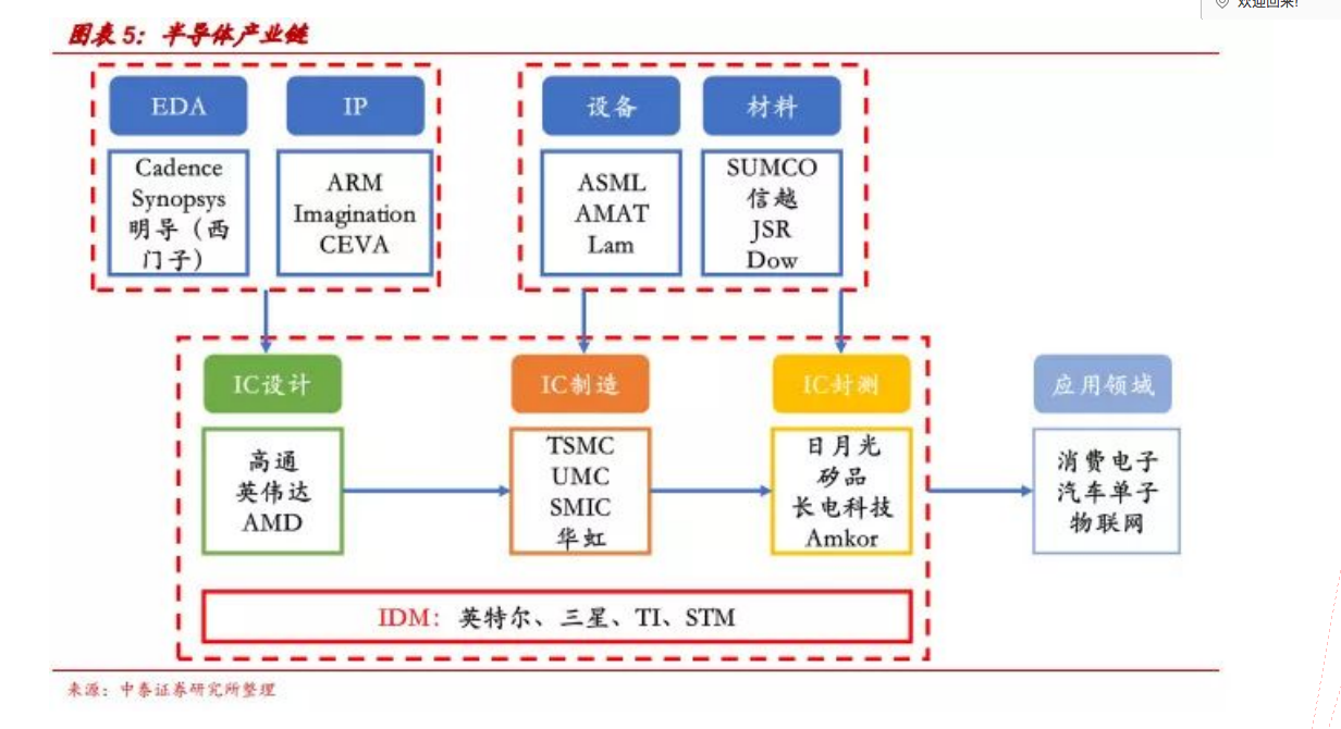
Semiconductor industry industry chain, picture from Zhongtai Securities
If a company wants to develop a chip, they will use the EDA tools provided by companies such as Cadence and Synospsys to assist in the design of the chip. After completion, it will be handed over to TSMC, UMC, SMIC and other foundries for production. The production equipment of these foundries includes lithography machines from ASML. Finally, after the packaging and testing of ASE and Changjiang Electronics Technology, a complete chip is formed.
It can be said that the main function of photolithography is to transfer the chip circuit diagram on the mask to the silicon wafer. It is the core link of IC manufacturing and the most complex and critical process step in the entire IC manufacturing.
2. Principle of lithography machine
Photolithography technology refers to the chemical change of photoresist under special wavelength light or electron beam, through exposure, development, etching and other processes, the design is The pattern on the mask is transferred to the pattern fine processing technology on the substrate.
The lithography machine generally writes directly on the photomask by laser or electron beam, and then irradiates the photomask with the laser. The photosensitive material on the wafer is Photosensitive changes in material properties, through development, complete the transfer of the chip from the design layout to the silicon wafer. This is actually very much like a camera + projector combination, but in the end I hope to print the circuit diagram on the silicon chip.
Let’s take a lithography machine with a laser as the light source as an example to see its simple working principle and process. When manufacturing a chip, first apply photoresist to the surface of the wafer (silicon wafer), and then irradiate the surface of the silicon wafer with light through the reticle (equivalent to the negative of the chip circuit drawing). The photoresist irradiated by the light will generate reaction. After that, the irradiated or unirradiated glue is washed away with a specific solvent, and the circuit diagram is printed on the silicon wafer.
3. Why is the lithography machine so important to the chip industry?
From the above, it cannot be seen that in the IC manufacturing link, the lithography machine is at the forefront of the previous processPart of it.
Generally speaking, the performance of a chip is affected by the density of transistors. The more transistors in the same area, the smaller the transistor line width , The stronger the chip performance. Among the nanometer processes we hear every day, the nanometer represents the line width of the transistor that can be processed by the corresponding lithography process.
Therefore, it can be said that the advanced performance of the lithography machine, to a certain extent, represents the advanced performance of the chip Sex.
2. Why is it so difficult to develop the most advanced lithography machine? ——Infinitely approach the limits of physics, materials science, and precision manufacturing
In February 2020, ASML, the world’s leading lithography machine, announced that it may launch a new generation of EUV lithography machine EXE:5000 series as early as 2021. This means that it is possible to produce chips with 3nm and 2nm processes. Before this, the most advanced lithography machine at the moment was launched by ASLMNXE : 3400C, the numerical aperture of the objective lens system is 0.33, which can support chip manufacturing of 7nm and 5nm process.
In fact, the cost of researching and developing these two machinesis probably no less than tens of billions of dollars, plus the time-consuming preparatory work It also lasted more than ten years.
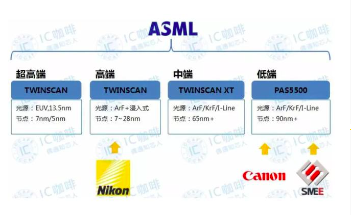
lithography machine classification
(1) How difficult is the most advanced lithography machine?
In order to more vividly quantify the difficulty of the most advanced EUV lithography machine, we can first talk about a few intuitive data:
-
An EUV lithography machine generally has more than 100,000 parts, 40,000 bolts, more than ten kilometers of wiring, and several hundred tons of weight;
-
An EUV lithography machine generally requires about 4 Boeing 747s to complete the transportation;
-
In 2015, the price of an EUV lithography machine was as high as 120 million US dollars;
-
At present, the well-known lithography machine company ASML has 25,000 employees, about 9,500 R&D personnel, 2,300 Ph.Ds, and about 60,000 supplier technical partners, and it needs to invest 10-15% annually Revenue is used as R&D investment.
How difficult is each chip process improvement? 1nm is approximately equivalent to one-fifty thousandth of the diameter of a hair. To achieve such a precision increase, it is not difficult to imagine.
In the article “War of the Lithography Machine”, the author Jin Jiefan also made a metaphor, “Because the lithography accuracy is a few nanometers, EUV requires extremely high light concentration, which is equivalent to taking a flashlight. The light spot on the moon does not exceed one coin. The mirror required for reflection requires a length of 30cm and the fluctuation is less than 0.3nm, which is equivalent to the fluctuation of a railway track from Beijing to Shanghai not exceeding 1mm.”
It can be said that the current most advanced EUV lithography machine, its difficulty has infinitely approached the limit of physics, materials science, and precision manufacturing.
lithography machine
(2) Why is the current lithography machine difficult to develop?
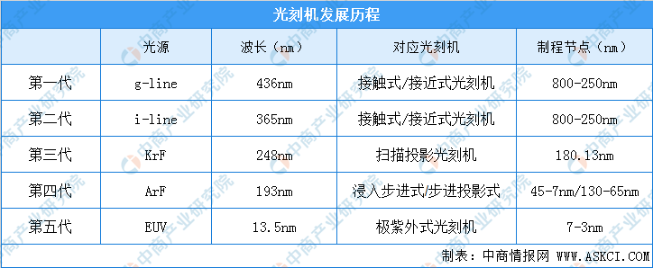
1. The evolution of the lithography machine is actually a process of continuously decreasing the wavelength
According to Moore’s Law,The number of components that can be accommodated on an integrated circuit, every It will double in 18 months. This means that the integration level of integrated circuit chips will increase approximately four times every three years, and the feature size of semiconductor devices will shrink approximately twice every three years.
As mentioned above, the performance of a chip is affected by the density of transistors. The more transistors in the same area, the smaller the transistor line width, the stronger the chip performance. We listen toAmong the several nanometer processes, the nanometer represents the line width of the transistor that can be processed by the corresponding photolithography process.
How can I increase the line width? here involved an important optical formula——Rayleigh’s formulaRayleigh Criterion.
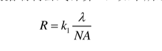
瑞Li formula
where R represents the smallest Half-angle resolution; K is a constant related to experience, generally determined by photolithography process, such as photoresist and mask pattern shape; λ represents the wavelength of incident light;NA represents the numerical aperture of the exposure system, and the value of NA is usually between 0.25-1.35.
If the lithography machine wants to reduce the transistor line width, it needs to increase the lithography resolution, That is, the R value in the formula should be low enough, which means to reduce the wavelength (that is, to reduce the λ value), to improve the process level (that is, to reduce the k value), and to increase the numerical aperture of the exposure system (that is, to increase the NA value). In the past few decades, the industry’s common practice is to reduce the wavelength (lower the λ value), that is, to develop a shorter wavelength light source that can be used in lithography machines.
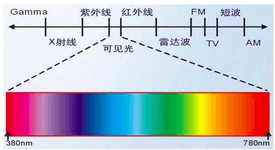
Spectrum
It can be said that in the past few decades, the light source of the lithography machine has been infinitely approaching the leftmost side of ultraviolet rays from the far right side of the infrared rays. The so-called EUV extreme ultraviolet lithography machine today uses the leftmost spectrum of the ultraviolet band.
In “War of Lithography Machines” also describes this process in detail:In the first half of the 90s, lithography began to use the wavelength 365nm i -line, the 248nm KrF laser was used in the second half of the period; among them, the 193nm wavelength DUV laser (the ArF excimer laser that became famous because of the difficulty) was used in lithography in the 2000s.
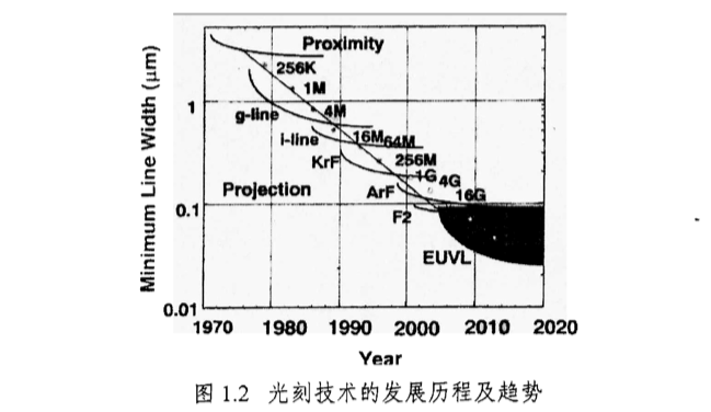
The development history and trend of lithography technology
When the lithography machine first appeared on the scene, the light source used a high-pressure mercury lamp g-line with a wave length of 436 mn, and the NA value was 0.28 to 0.30. In the first half of the 1990s, the light source I started using the 365nm i-line at the moment, and the NA value is 0.50-0.55. Take the memory chip as an example. It is mainly used for 16MibtDRAM manufacturing process. In the latter half of the 1990s, 248nm KrF lasers began to be used, with an NA value of about 0.60. Taking the memory chip as an example, it is mainly used in the manufacturing process of 64 Mibt DRAM and 256 Mibt DRAM. In the 2000s, lithography began to use DUV lasers with a wavelength of 193nm (the ArF excimer laser, which became famous because of its difficulty).
The EUV that often appears in the news now is extreme ultraviolet, with a wavelength of 13.5nm. According to the introduction of the author ArtoriasPhD , here is an interesting digression. The reason for skipping from 365nm, 248nm, 193nm on the progress bar 157nm, directly to EUV with a wavelength of 13.5nm, one of the main reasons is that 157nm will be absorbed by most of the lenses, severe heat will cause the mirror surface to deform, and the reflection and focus cannot be accurately reflected. =”letter-spacing: 0px;”>Use fluorite calcium fluoride to make the lens, but the cost is very high and only Canon has the manufacturing technology of some small fluorite lens, and finally gave up after a few years.
2, useLow wavelength light source
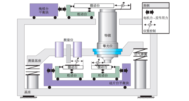
A typical lithography machine system structure is shown in the figure above, including the following four parts: light source; illumination system; projection optical system; workbench.
Generally speaking, the light waves emitted by the light source are projected onto the reflective mask through the multilayer film mirror of the illumination system, and the reflected light waves are then passed through the surface mirror optical miniature projection system to integrate the reflective mask The circuit geometry is projected and imaged into the resist on the silicon wafer to form the lithographic pattern required by the integrated circuit.
The use of low-wavelength light sources will not only bring about changes in the lighting system, projection optical system, and workbench, but also bring new challenges to materials.
We take the EUV lithography machine, which has the most attention at the moment, as an example to disassemble it.
To ensure the lithography work, first of all, it is necessary to ensure the “ability” of the light source and the final accurate projection after multiple reflections. Therefore, to ensure the required capabilities of the lithography machine, a qualified light source must first be manufactured. Taking ASML as an example, in order to solve the problem of light source manufacturing, it acquired Cymer, the world’s leading supplier of excimer lasers. The so-called qualified here refers to the realization of narrow-band EUV output of specific power at an appropriate cost.
Secondly, it is necessary to design a special lens to ensure that the light source is concentrated by continuous reflection and the lens absorbs the light energy. There is a statistical data that shows that for every reflection, the EUV energy will lose 30%. After more than a dozen reflections, the light reaching the wafer is theoretically only 2 %. South Korean company Hynix once stated that the energy conversion efficiency of extreme ultraviolet EUV is only about 0.02%. If calculated according to this conversion rate, the output power of ASML’s EUV lithography machine is 250 watts, and the input power is likely to reach 1.25 million watts, which consumes 30,000 kWh per day. Therefore, the miniature projection optical system of the EUV lithography machine should be composed of as few mirrors as possible. This will reduce the free variables in optical design and limit the imaging quality of the optical system. For this reason, aspheric mirrors are generally used to increase the free variables in the design of the miniature projection optical system. However, the use of aspherical mirrors will produce distortion, and the distortion will lead to image misalignment, and ultimately lead to distortion of the mask copied pattern. Therefore, the projection system needs to have sufficient resolution to achieve minimal distortion.
Again, the mask lighting system with excellent performance and the excellent micro-projection optical system can work together. The mask illumination optical system is also considered to be one of the most important subsystems in the EUV lithography machine, which directly influences the performance of the entire device. The mask illumination optical system must meet such conditions at the same time: Collect the maximum energy possible from EUV Narrow-band EUV radiation, and form an annular illumination field of view matching the miniature projection opticssystem on the mask; at the same time guaranteeThe uniformity of the radiant illumination of the annular illumination field of view. This also means high demands on the craft.
In addition, materials are also an important difficulty. For example, in 248nm and 193nm, organic chemical amplification photoresist CAR is used. However, in the EUV era, because the energy of the light source increases significantly, the performance of CAR may be unstable, which affects the chip yield. And if it comes to X-ray lithography, new suitable lithography materials are needed.
(3) Another difficult problem in the development of lithography machines-funding
From the technical disassembly above, it is not difficult to guess. There is another problem in making a lithography machine-funding.
In fact, due to the technical difficulty of the lithography machine and the huge investment in research and development, Canon and Sony both suffered serious losses and have stopped research and development and withdrew from the future technology competition. The United States and other developed countries research lithography machines, almost every year more than 9 billion funds are used as research and development expenses. So far, these countries that master lithography machine technology have spent about 400 billion yuan.
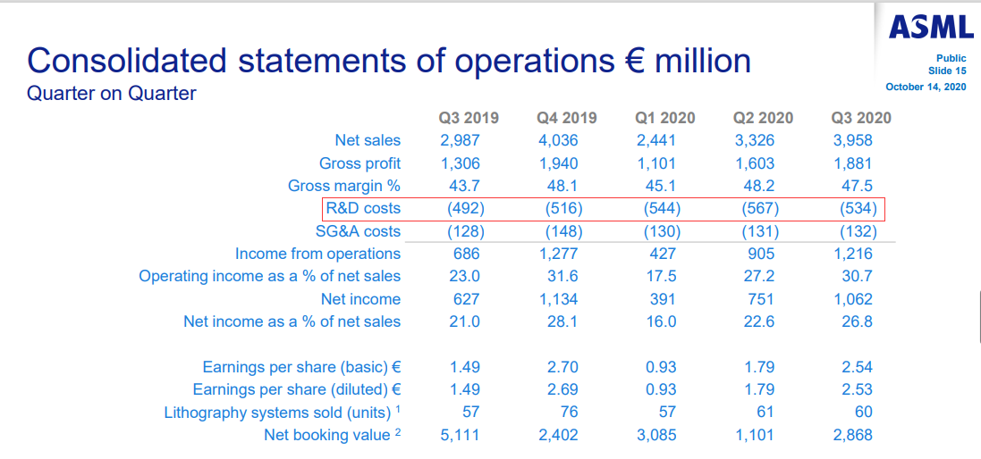
ASML Financial report, from ASML official website
ASML’s financial statements for the third quarter of 2020 released on October 14 show that ASML’s total revenue for the third quarter of 2020 was 3.958 billion euros, and research and development expenses were 534 million euros, accounting for approximately 13.49% of total revenue; Research and development expenses in the second quarter of 2020 were 567 million euros, accounting for approximately 16.87% of total revenue for the quarter; research and development expenses in the first quarter of 2020 were 544 million euros, accounting for approximately 22.28% of total revenue in the quarter. The total revenue for the whole year of 2019 was 11.8 billion euros, and the research and development expenses reached 2 billion euros, accounting for about 16.94% of the total revenue, which was a substantial increase from the 1.6 billion euros in 2018. ASML said: In the past five years, ASML’s R&D investment has reached 7 billion euros. According to e company reports, ASML has invested more than 1 billion euros in research and development every year, and it has only developed the latest lithography equipment-EUV lithography machine for 20 consecutive years.
At present, ASML, the leader of the lithography machine market, can almost be said to be the monopolist of the entire lithography machine technology. Their annual research and development expenses are almost the three-quarter income of some Fortune 500 companies. ASML, in order to raise funds, but also to bundle upstream and downstream interests and share R&D risks, it invites Intel, Samsung and TSMC to invest and become its major shareholders. ASML is actually a joint investment project of the United States, Japan, South Korea, Germany, etc., to ensure sufficient funds.
Three, the history of lithography machine
(1) Development of the Technology Route of Lithography Machine
1. Technological progress changes
The development history of lithography technology Source: China Business Intelligence Bureau
Driven by Moore’s Law, optical lithography technology has undergone five generations of changes. From the 1970s to the 1980s, lithography equipment mainly used ordinary light sources and mercury lamps as exposure light sources, with feature sizes above the micron level. The first exposure wavelength was from the g-line at 436nm to the i-line at 365nm in the first half of the 1990s, and the KrF laser at 248nm in the second half. After entering the 21st century, the lithography technology began to use the DUV laser at 193nm. This is the famous ArF excimer laser, which technically spans 1μm, 0.5μm, 0.35μm, 0.1μm, 90nm, 65nm, 45nm and other nodes. At present, the latest lithography technology is EUV (Extreme Ultraviolet Lithography Machine), the wavelength is also shortened to 13.5nm, and the process node is also increased to 7-3nm. At present, optical lithography technology is moving in the direction of shortening the wavelength of the exposure light source, increasing the numerical aperture and improving the exposure method.
2, 193nm lithography: a technological breakthrough that rewrites the historical commercial pattern
When it comes to lithography machine technology, I have to mention the 193nm technological breakthrough. From the result point of view, the immersion technology that exceeds the 193nm wavelength turned out to be a leader in the field of lithography machines, and also ushered in the next era of lithography machines-the EUV era. But the hardship of the whole process runs through the 90s of the world.
In the 1990s, the light source wavelength of the lithography machine was stuck at 193nm, which became a difficulty for the entire industry. Scientists and the industry have proposed various solutions beyond 193nm, including the 157nm F2 laser advocated by Nikon and other companies, and the EUV LCc alliance bet more radical EUV (13.5nm), Japanese company and IBM supported X-ray, electron beam projection (EPL), ion projection (IPL) and other technologies.
At this time, TSMC’s top class in 2002Lithography expert Lin Benjian developed the 193nm immersion lithography technology using water as the medium: the medium between the lens and the silicon wafer is changed from air to water. Since the refractive index of water is about 1.4, the wavelength can be shortened by 132nm. Although this idea was initially rejected by various semiconductor giants, after all, this is just an ideal situation. Adding water to a sophisticated machine to build an infiltration environment requires consideration of actual performance and concerns about environmental pollution.
However, ASML, who was “being not afraid of tigers” at the time, chose to gamble with Lin Benjian, betting that the immersion technology could be developed in a small way. In the following year, ASML and Lin Benjian developed the first prototype And successively won orders from major customers such as IBM and TSMC. Although Nikon also launched a dry lithography 157nm technology product soon afterwards, ASML seized the opportunity, and its wavelength technology is not as good as ASML, so it is commercially available It is not dominant.
Because I won the bet in the technical dispute between 157nm light source dry engraving method and 193nm light source wet engraving method, ASML realized a curve in the field of lithography machine Overtaking, the field of lithography machine not only changed a leader, but also ushered in the next era of lithography machine-EUV era.
I can add a little bit here. According to the light source of the lithography machine, the lithography machine can be divided into ultraviolet light source (UV), deep ultraviolet light source (DUV), and extreme ultraviolet light source (EUV). Relationship, the wavelength is getting smaller and the resolution will be higher and higher. The conventional DUV lithography machine uses 193nm deep ultraviolet light, and the current EUV lithography machine uses extreme ultraviolet light with a wavelength of 13.5nm. With the birth of EUV technology, chip production in 14nm, 10nm, and 7nm processes has been realized, and through technological upgrades, chip production in 9nm, 8nm, 6nm, 5nm, 4nm and even 3nm processes can also be realized.
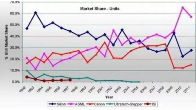
1992-2011 market share of major companies in the field of lithography machine pictures from the Internet
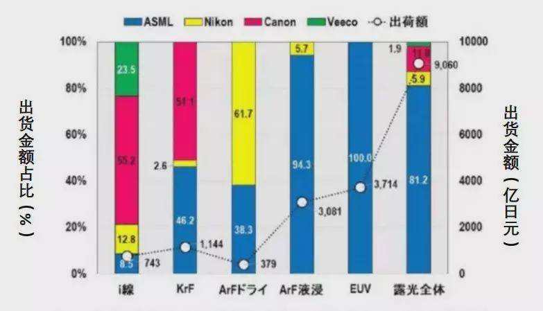
2019 global shipment amount of various exposure equipment and the proportion of each shipment amount Source: China Machinery Community
(2) How ASML became today’s most important lithography player
1. ASML financial data
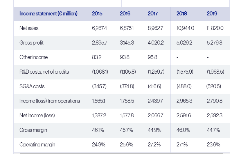
ASML financial report (partial) data for the past five years
According to the financial report data disclosed by ASML in the past five years, ASML’s net sales and net income have shown an upward trend in the past five years, especially in 2016-2018, ASML’s revenue has risen sharply. As of the end of 2019, ASML’s R&D expenditure has reached 2 billion euros a year, which is not the scale of funds that an ordinary company can raise in a short period of time. According to the introduction of Zhihu users, in the early days of ASML’s slow development, in order to maintain the technological leadership, fundraising for research and development funds was carried out in the name of the “Customer Joint Investment Plan”: customers exchanged capital for the priority ordering rights of EUV lithography machines. Assist customers to increase product output. Through this plan, ASML uses 23% of its equity to obtain 503 million euros in equity investment from Samsung and 275 million euros in R&D support, TSMC’s 838 million euros in equity investment, and long-term partner Intel’s $4.1 billion equity and $1 billion. R&D support has ensured its dominant monopoly position.
ASML has long been ahead of industry rivals in R&D expenses. For a long time, its R&D expense/total sales ratio has been stable at around 20%, far exceeding the industry average of 3%. In addition, ASML holds a large amount of cash for a long time to ensure that R&D expenses are not affected by the economic cycle. It is precisely because of a large amount of investment in research and development that ASML has now maintained its first position in the industry in terms of lithography technology.
The technical barriers of ASML are obvious, while the ecological barriers areIts invisible moat.
In the early days, ASML joined the EUV LLC alliance jointly established by the U.S. Department of Energy and Intel, sharing top technology, talents and resources with the then leading technology companies such as AMD and Motorola. This can be understood as “making good bonds” in the ecology of others.
In the later period, ASML relied on the upstream and downstream relationship to build its own ecology. ASML CEO Peter Wennink once mentioned, “ASML is a system integrator that integrates the technologies of hundreds of companies, and a lithography machine requires 80,000 parts.” . And because of the precision and complexity of its products, and because of its high capital intensiveness, ASML had to share technology with some upstream and downstream partners, and even let some of them become their own shareholders.
Four. History of lithography machine
(1) History of China’s Lithography Machine Development
Following the context of time, let us walk into the first era of Chinese lithography machines.
The development history of my country’s lithography machine can be traced back to the 1950s. In 1956, my country’s first transistor was born. Since then, China’s semiconductor industry has entered a new era. Then, in 1958, the first germanium The transistor was successfully trial-produced. In 1962, the first generation of silicon planar transistors (transistors made with planar technology) came out. In 1966, 109 Factory cooperated with Shanghai Optical Instrument Factory to successfully develop my country’s first 65-type contact lithography machine.
With the rise of research in the semiconductor industry, China successfully developed the first lithography machine belonging to China in 1977—GK-3 semi-automatic lithography machine. According to relevant data, this is a contact lithography machine. Engraved machine. The following year was 1978, at the time of reform and opening up, my country developed GK-4 on the basis of GK-3, and also increased the diameter of the processed wafer from 50nm.At 75nm, the degree of automation has improved a lot, but the contact lithography machine is still not getting rid of. In the same year, the Institute of Semiconductors of the Chinese Academy of Sciences began to develop the JK-1 semi-automatic proximity lithography machine. In 1980, Tsinghua University developed the fourth-generation step-by-step projection lithography machine with a lithography accuracy of 3 microns. In 1981, the Institute of Semiconductors of the Chinese Academy of Sciences successfully developed the JK-1 semi-automatic proximity lithography machine. In 1982, the 109 Factory of the Academy of Sciences successfully developed the KHA75-1 semi-automatic advanced contact lithography machine. In 1985, the 45th Institute of the Mechanical and Electrical Department successfully developed a prototype of the BG-101 step lithography machine, which was the first step projection lithography machine in China.
In the early 1980s, it can be said that China’s early lithography machines accelerated the development of a few years and worked hard to shorten the gap between China and foreign countries. However, in the middle and late 1980s, with the deepening of reform and opening up, on the one hand, large-scale foreign investment began to be introduced. The idea of “buying is better than making” has emerged in the machine industry. In essence, it has given up independent research. And due to the characteristics of the times, the country attaches great importance to the fast-growing industry. However, lithography machines, such projects that require long-term high investment, are gradually being marginalized. The development and industrialization of lithography machine technology has stagnated due to the lack of national attention. On the other hand, in the article “Review of the History of the Development of Domestic Lithography Machines”, it is written that the western developed countries have restricted my country’s lithography machine technology and restricted the export of lithography machine-related accessories to my country. Due to these two reasons, China, which can finally be expected, will begin to lose touch with foreign countries again. Until the 1990s, the light source of my country’s lithography machine had been stuck at 193nm for more than 20 years.
In the 21st century, taking advantage of the development of China’s semiconductor technology, lithography technology has regained the attention of the country and gradually began to develop. my country has also started the 193nmArF lithography machine project. In 2002, Shanghai Microelectronics Equipment Co., Ltd. was established. This company has played a pivotal role in the history of China’s lithography machine development. Just after its establishment, it undertook the national “Tenth Five-Year Plan” lithography machine research project. In 2008, the “Very Large Scale Integrated Circuit Manufacturing Equipment and Complete Processes” project listed ASML’s EUV technology as a key direction for next-generation lithography technology. The country plans to realize the localization of EUV lithography machines in 2030. In 2016, Shanghai Microelectronics has mass-produced three lithography machines of 90nm, 110nm and 280nm. In 2017, the “Key Technology of Extreme Ultraviolet Lithography” led by Changchun Institute of Optics, Fine Mechanics and Physics, Chinese Academy of Sciences passed the acceptance. In 2018, the “super-resolution lithography equipment” developed by the Chinese Academy of Sciences passed the acceptance. The lithography resolution reaches 22 nanometers, and combined with double exposure technology, it can also be used to manufacture 10 nanometer-level chips in the future. It is reported that
At the beginning of June 2020, Shanghai Microelectronics announced that it would deliver the first 28nm process domestic immersion lithography machine in 2021-2022. The domestic lithography machine is expected to break through the previous 90nm process to 28nm process, but in reality The most advanced ASML company in the world is stillThere is a gap of about 20 years.
2, the gap between China and foreign countries
When the first transistor was invented in China, it has been nine years since Bell Labs developed the world’s first fulcrum contact transistor. The United States has developed a contact lithography machine in the 1950s, while China only developed the first lithography machine in 1977, the GK-3 semi-automatic lithography machine. During this period, there was a difference. For more than twenty years.
But in the 1980s, the gap between China’s research level in the field of lithography machines and foreign countries gradually narrowed. Relevant data shows that the fourth generation developed in the 1980s The lithography accuracy of the stepwise projection lithography machine has approached the international mainstream level. The KHA75-1 semi-automatic proximity contact lithography machine in 1982 has reached the level of Canon PLA500-F in some important indicators (such as mask deformation, etc.). The BG-101, China’s first step lithography machine developed in 1985, made the gap between China and foreign countries no more than 7 years in the step lithography machine, greatly shortening the gap between China and foreign countries.
Due to the lack of attention in the mid to late 1980s and technical limitations, the newly shortened distance has to be enlarged. In the 1990s, ASML had begun the research and development of EUV lithography machines, but it was not until the 21st century that China had just started the 193nmArF lithography machine project, which was more than 20 years behind ASML.
After entering the new century, China’s lithography machine business has received national attention and has developed to a certain extent. However, since my country has been purchasing from overseas before 2018 As far as lithography machines and semiconductor chips are concerned, the development of my country’s lithography machine industry has always been in a state of unhurried and tepid. The gap with the world’s leading R&D level has not been effectively narrowed, but is just The stage of running. At present, there is still a gap of about 20 years between China and the world’s most advanced ASML company in the field of lithography.
Here is a quote from Boss Dai in Chaoyang District who knows the user: “From the current reality of the world’s lithography machine industry, there are only 3 contestants in front of Shanghai Microelectronics Equipment Co., Ltd., and the Dutch ASML, Japan’s Canon and Nikon. If the score is purely based on numbers, if ASML is 100 points, Canon is about 20 points, Nikon is about 25 points, and Shanghai Microelectronics is about 5 points.”
It can be said,The gap between China and foreign countries is still a long way to go, and it is still necessary to “we will search up and down.” The development of China’s lithography machine is still very long and requires investment from all aspects of capital, technology, talents, enterprises, and the government.
V. International lithography machine industry pattern
Source: China Business Industry Research Institute
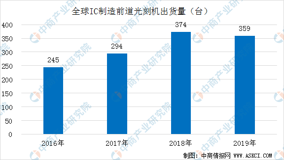
According to data from the China Business Industry Research Institute, from 2016 to 2018, the global sales of front-end lithography machines for global IC manufacturing were on an upward trend. In 2018, global shipments reached 374 units. Shipments declined slightly in 2019 to 359 units for the whole year.
From the perspective of the competitive landscape, at present, according to the three major companies in the global lithography machine market, namely ASML, Nikon and Canon, ASML accounts for about 75% of the global lithography machine market industry structure, and Nikon accounts for about 13%. , Canon accounted for about 6%, and other companies accounted for about 7% of the total.
Source: China Business Industry Research Institute
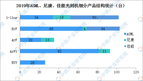
From the perspective of lithography machine sales, the combined market share of the three companies in 2019 accounted for more than 90% of the global lithography machine market. According to China Business Intelligence Network, the main products of ASML in the Netherlands are lithography machines of various levels. In 2019, ASML sold 229 lithography machines, of which ArFi lithography machines accounted for the largest proportion, and the market accounted for 88%; followed by KrF lithography machine, the market share is as high as 71%, and it is worth mentioning that the market share of ASML’s EUV lithography machine can reach 100%, completely monopolizing the entire market. Nikon is currently mainly mid-to-high-end models, including ArF, KrF, KrF, and i-line light sources. The immersion lithography machine was launched after ASML. It used to be the first in the field of lithography machines, but it is now behind ASML. Canon focuses on low-end products, only i-line and Kr-F lithography machines, no immersion lithography machine, now Canon has gradually reduced the field of semiconductor lithography machineInvestment in the field of panel lithography machines.
In the field of domestic lithography machines, Shanghai Microelectronics takes the lead. As the leading lithography machine research and development company in China, it is also the most competitive enterprise in China. Its products mainly use ArF, KrF and i-line light sources. , It can only reach 90nm process at present, and it is mainly used in IC back-end packaging and panel field.
VI. Future development trend of lithography machine
(1) The future lithography machine is still not a big market
Today, 2nm and 3nm lithography machines are the most concerned by everyone, mainly in the field of mobile phone chips, but in fact, the previous larger process lithography machines are still on sale, and the sales are good. From the perspective of industry supply, from 2014 to 2018, the top three companies (ASML, Nikon, Canon) in the field of lithography machines showed a fluctuating growth in sales. In 2019, the sales volume of lithography machines declined, with global sales of 354 units, a decrease of 3.8% from 2018. In the first quarter of 2020, the sales volume of the top three companies in the field of global lithography machines reached 85 units. In addition to the lithography machine used in the front line of IC, the niche market of package lithography machine and LED/MEMS/power device lithography machine is also constantly developing. Data from the “Market Competitiveness Analysis and Investment Prospects Report of China’s Lithography Machine Industry in 2020-2026” released by Zhiyan Consulting shows: From the perspective of demand, the market demand for advanced packaging lithography machines is greater and the growth rate is the highest. The main driving force of the base market. The shipment volume of advanced packaging, MEMS and LED lithography machines will continue to grow from 2015 to 2020, and the total demand is expected to exceed 250 units per year by 2020. But the overall scale is only in the demand for hundreds of units per year, so the future lithography machine will still not be a big market.
(2) X-ray lithography machine is still unable to achieve engineering mass production for the time being
In the field of semiconductor industry, X-ray lithography machine technology is also researched lithography technology. According to what I know as a user, I’m a technology mad, today’s EUV extreme ultraviolet lithography technology is relatively mature, with good optical characteristics and good economy. The wavelength of X-rays ranges from 0.001 nm to 10 nm. The smaller wavelength means that the diffraction of light waves can be reduced, which is conducive to the formation of tiny and clear images. The X-ray lithography machine technology has better penetrability, can be formed with a higher aspect ratio, and manufacture next-generation 3D transistors and smaller nanometer chips.
Now companies that use X-ray lithography mainly use LIGA technology, a technology used to manufacture high aspect ratio structures, which can produce a 100:1 aspect ratio.In mems technology. However, the biggest problem of X-ray lithography technology is precisely because its penetrability is too strong, which makes it impossible to zoom in and out with the lens. Therefore, the size of the pattern is the same as the size of the mask. For example, a pattern of 100nm size needs a size of 100nm. Reticle, so X-ray lithography relies too much on the accuracy of electron beam lithography reticle, so it is not widely popularized at present. At present, the minimum accuracy made by X-ray is 30nm, this accuracy is not high enough in the middle, the accuracy of CMOS devices is far from enough, and the small size is not needed for mems, and the cost is not cheap.
Previously, ASML experts said offline that EUV can at least iterate forward by at least one generation, and there is the possibility of iterating two generations. This will have a cycle of at least 10 years. From economic considerations, EUV light The engraving machine may be able to support 2nm and 1.4nm processes.
(3) Small chip Other supplementary solutions for miniaturization
The miniaturization and miniaturization of chips is an irreversible trend. The advancement of lithography machines represents an advanced process. In addition to this, the industry is also actively looking for other ways to keep the chip small while maintaining the high performance of the chip. On the whole, there are several major ideas in the direction of chip miniaturization, including:geometric miniaturization,Circuit miniaturization,device miniaturization,architecture miniaturization. Each program also has some scientific research and industrial progress. As we often hear of 3D packaging, 2.5D packaging, etc., all appeared in this context.