The polarization array waveguide scheme and the embossed grating waveguide scheme are currently the two most promising mainstream AR schemes, one for the present and one for the future.
Editor’s note: This article comes from the WeChat public account “Long Jing Photoelectricity” (ID: Lochn2014) .
1, Introduction
Augmented reality technology, or AR technology, is the fusion of virtual information and the real world. It is the tipping point of the next information technology. According to authoritative predictions, augmented reality glasses will replace mobile phones as the next generation of collaborative computing platforms. Augmented reality technology represented by augmented reality glasses is currently emerging in various industries, especially in the security and industrial fields. Augmented reality technology embodies unparalleled advantages and greatly improves the way of information interaction.
At present, the more mature augmented reality technology is mainly divided into prism scheme, birdbath scheme, free-form surface scheme, off-axis holographic lens scheme and waveguide (Lightguide) scheme. The first three schemes are relatively large, It limits its application in smart wearables, namely augmented reality glasses. The holographic lens scheme uses the unique optical characteristics of the hologram, which has the advantages of large FOV and small volume, but is limited by the relatively small range of eye movement.
Waveguide is currently the best augmented reality glasses solution . The waveguide scheme is divided into geometric waveguide scheme, relief grating waveguide scheme and volume holographic waveguide scheme . The geometric waveguide scheme generally includes a sawtooth structure waveguide and a polarized film array mirror waveguide (referred to as a polarized array waveguide for short). Among them, the mainstream polarization array waveguide uses the partially transmissive and partially reflective thin film mirror of the array to achieve the purpose of displaying virtual information. The polarization array waveguide scheme has the advantages of light and thin, large eye movement range and uniform color. Relief grating waveguide solutions can be mass-produced using nanoimprint technology, which has caused great interest from AR optical module manufacturers. It has the advantages of large field of view and large eye movement range, but it also brings uniform field of view Challenge of uniformity and color uniformity, and related micro-nano processing technology is also a huge challenge. The volume holographic waveguide scheme has advantages in color uniformity (no rainbow effect) and realization of a monolithic full-color waveguide, but it is currently limited in large-scale mass production and a large field of view.
Figure 1 is the basic display principle of the waveguide scheme. The coupling area is used to couple the light beam of the micro-projector into the waveguide plate, so that the beam meets the conditions of total reflection propagation in the waveguide plate, and the coupling area is used The light beam propagating through the total reflection is coupled out of the waveguide plate and reaches the human eye. The coupling region can beMirrors, prisms, relief gratings, volume holographic gratings, etc. The decoupling area may be an array semi-transparent mirror, a relief grating, a volume holographic grating, and so on. This article will further explain the waveguide scheme and the diffractive waveguide processing technology, and introduce the research and development of Longjing Optoelectronics in this field.
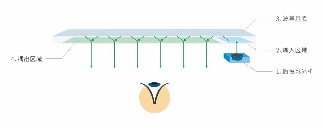
Figure 1: Schematic diagram of waveguide scheme
2. Geometric waveguide scheme
2.1 Sawtooth waveguide
The basic principle is to use a zigzag reflecting surface with a certain reflectivity at the position in front of the eyes to couple light reflection out to the human eye.
Figure 2: The first type sawtooth waveguide optical module diagram
Figure 3: The second type sawtooth waveguide optical module diagram

Figure 4: Partial zigzag structure diagram
Figure 2 is a structure with a serrated bevel [1]. The structure of the bevel is shown in Figure 4. The virtual image transmitted in the waveguide sheet is reflected from the zigzag structure into the human eye, and the external ambient light passes through the two complementary zigzag structures directly into the human eye without being affected. The structure of Fig. 3 utilizes the intermittent sawtooth structure [2] to complete the merging of the virtual image and the external environment image. However, the more teeth in this structure, the more stray light will affect the contrast and reduce the image quality. Moreover, the light is coupled to the human eye only after one reflection on the sawtooth structure, and it will become stray light more than once. If you want to improve this effect, you must increase the thickness of the waveguide. At the same time, coating on multiple sawtooth structures undoubtedly increases the process difficulty. Figure 3 The problem with the structure is that the energy utilization rate is relatively low, because some of the non-sawtooth structure cannot fully reflect the energy. Even if the non-reflected part is blocked by a certain angle of deflection, the full field angle cannot be taken into account. The energy loss is particularly noticeable.
2.2 Polarized array waveguide
Lumus products are shown in Figure 5 (a) [3]. This method has obvious advantages compared to the above sawtooth waveguide. His reflective structure covers the entire waveguide sheet. The position of the waveguide lens in the middle has an angle-selective partially transparent and partially reflective film surface arranged in an array. Therefore, we usually call this a polarization array waveguide technology. Because there are multiple partially transmissive and partially reflective surfaces, each surface will reflect part of the light out of the waveguide and enter the human eye, and the remaining light will pass through and continue to advance in the waveguide. Then this part of the advancing light encounters another mirror, repeating the above “reflection-transmission” process until the last mirror in the mirror array reflects all the remaining light out of the waveguide into the human eye. As shown in Figure 5 (b), multiple reflections can “adjust” the emitted light to be more uniform.
Figure 5: (a) Lumus polarization array waveguide product diagram;
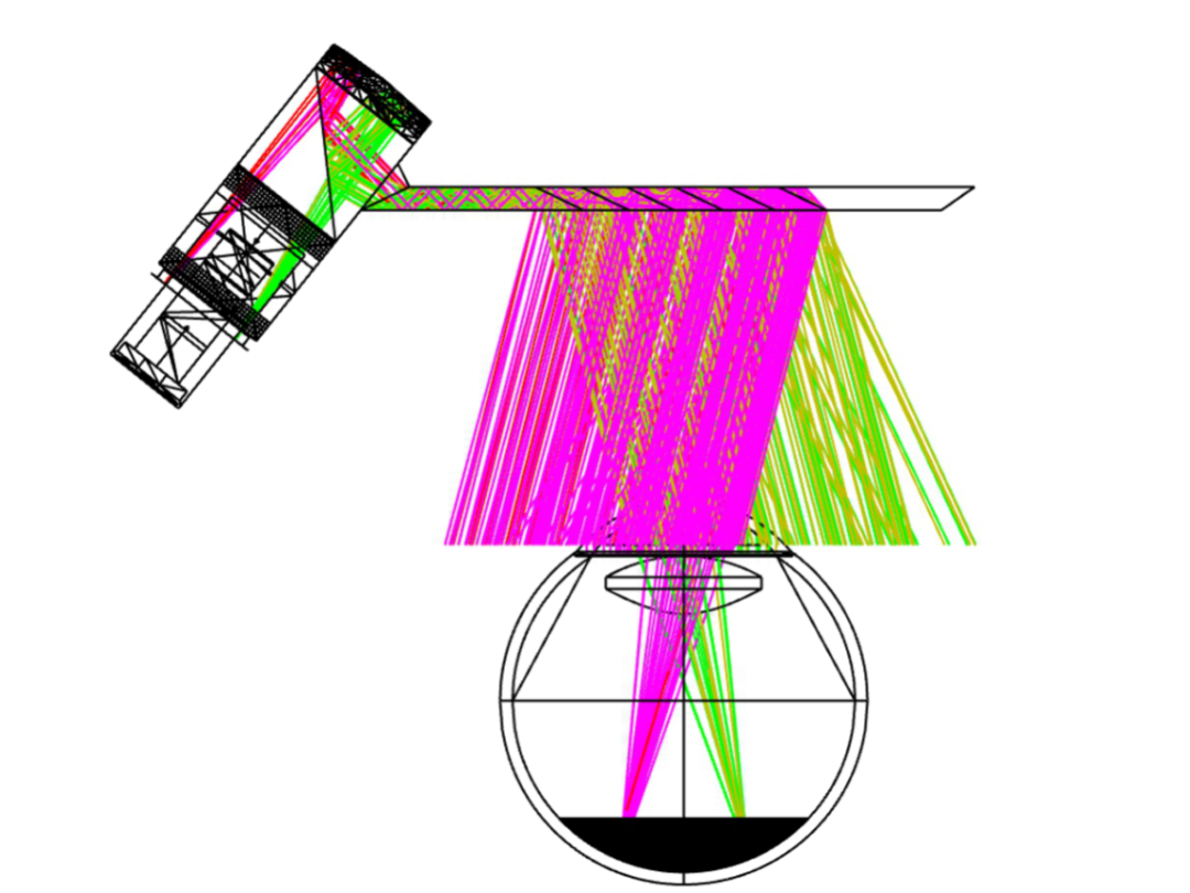
Figure 5: (b) Longjing Photoelectric Polarization Array waveguide optical path diagram.
The pupil dilation technology of this technology is more complicated in design. Stray light, human eye compatibility, and various performance indicators must be fully considered during design. In addition, uniformity is also an intuitive indicator of the end user experience. How to control the reflection and transmittance of multiple layers, how to optimize the whole machine, and how to control the coating process to ensure uniformity in the entire eye movement range, also The focus of the research. To this end, Long Jing Optoelectronics has developed a toolbox for polarized array waveguide design software, which makes the design of waveguide sheets more intelligent (one-button design). Technology independently developed optical processing technology, so that performance and cost have advantages. Figure 6 (a) shows the 3D simulation optical path diagram of Longjing photoelectric polarization array waveguide. Figure 6 (b) shows a picture of a polarization array waveguide product of our company.
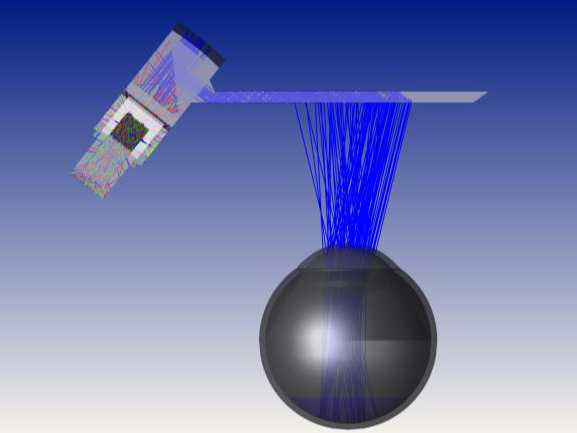
Figure 6: (a) Longjing photoelectric polarization array waveguide 3D optical path diagram;
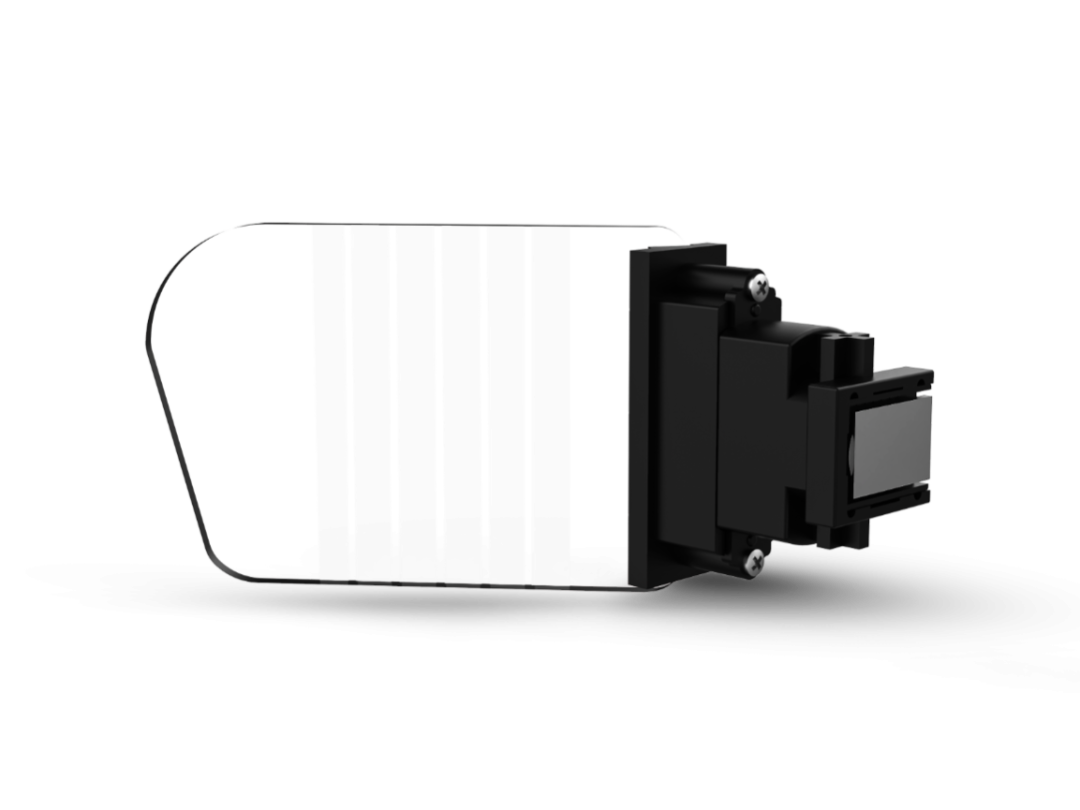
Figure 6: (b) Longjing Photoelectric Polarization Array Waveguide Products;
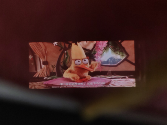
Figure 6: (c) Longjing Photoelectric Polarization The actual effect diagram of arrayed waveguide products.
3. Relief grating waveguide solution
The relief grating waveguide scheme is to use the relief grating (SRG) instead of the traditional catadioptric optical device (ROE) as the coupling scheme in the waveguide scheme, coupling out and out pupil expansion device. Commonly used relief gratings mainly include one-dimensional gratings, including inclined gratings, trapezoidal gratings, blazed gratings and rectangular grating structures. Figure 7 (a) shows the scanning electron microscope (SEM) images of inclined gratings. A two-dimensional grating, such as a hexagonal cylindrical grating structure commonly used in waveguides, Figure 7 (b) shows an SEM image of the two-dimensional cylindrical grating structure. The feature sizes of the above grating structures are all on the nanometer scale.
So the current route of the relief grating waveguide mainly includes: a relief grating waveguide scheme based on a one-dimensional grating. The schematic diagram is shown in Figure 8 (a), which is divided into coupling, turning, and coupling out regions. The one-dimensional grating is expanded in one direction at the turning area and the decoupling area, respectively, and the representative product is HoloLens. Relief grating waveguide scheme based on two-dimensional grating,The schematic diagram is shown in Figure 8 (b), which is divided into coupling-in and coupling-out regions. The classical structure of the coupling-in region is a one-dimensional grating, and the structure of the coupling-out region is a two-dimensional grating, using multiple levels of the two-dimensional grating structure. At the same time to ensure the coupling of the beam and the expansion of multiple directions, the representative company is WaveOptics. Fig. 8 (c) is the K-domain diagram of the two-dimensional grating waveguide. The inner circle represents the total reflection condition in the waveguide plate, and the outer circle represents the maximum K value that can be achieved by the material of the waveguide plate. The coupled K grating translates the K value of the beam to The ring-shaped area, that is, the beam meets the conditions for total reflection propagation in the waveguide plate, the coupling-out grating translates the K value of part of the beam from the ring-shaped area to the inner-circle area, that is, the beam is coupled out to the human eye.
Figure 9 (a) shows the first generation of relief grating waveguide designed by Long Jing Optoelectronics. The two-dimensional grating waveguide solution used by Long Jing Optoelectronics. The relief grating waveguide with independent intellectual property rights of Long Jing Optoelectronics is also being developed and perfected. As shown in Fig. 9 (b) and Fig. 9 (c), they are the field tracking simulation results based on the two relief grating waveguide principles made by our company.
Figure 10 (a) is the effect picture of Microsoft’s latest Hololens2 [4], Figure 10 (b) is the effect picture of WaveOpics diffraction waveguide [5], and Figure 10 (c) is the effect picture of Dispelix diffraction waveguide [6] ]. These three companies are currently representative companies in relief relief waveguides abroad.
The relief grating waveguide uses the photolithography process to process the wafer as a master, and uses the nano-imprint process for large-scale replication and mass production. See below for details.
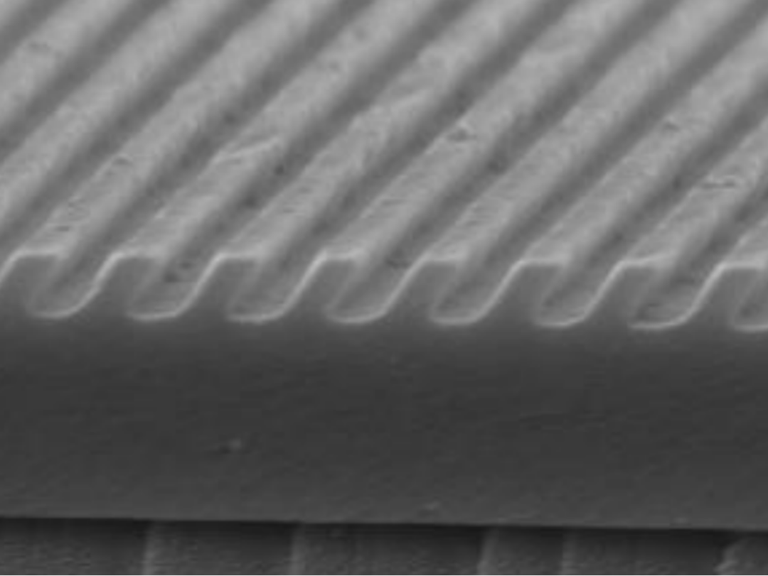
Figure 7: (a) inclined grating structure diagram;
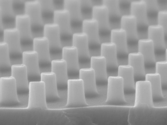
Figure 7: (b) 2D cylindrical grating Structural drawing.
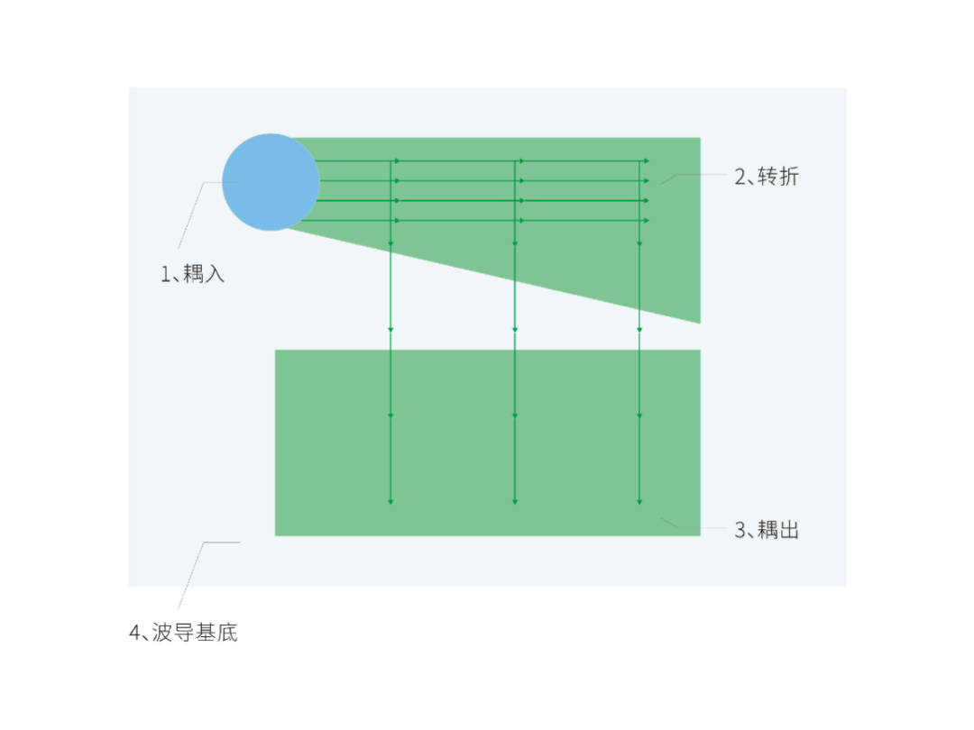
Figure 8: (a) Schematic diagram of one-dimensional grating waveguide;
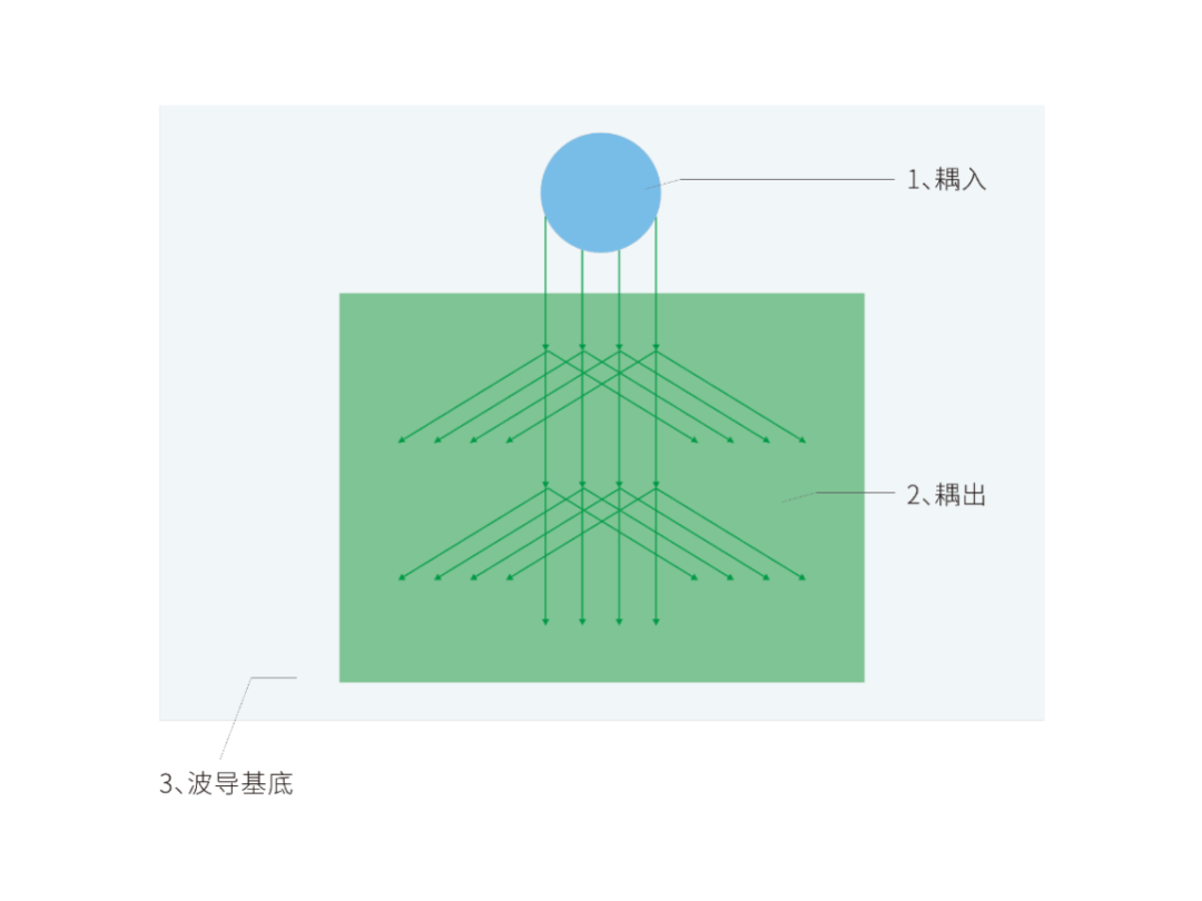
Figure 8: (b) Schematic diagram of two-dimensional grating waveguide;
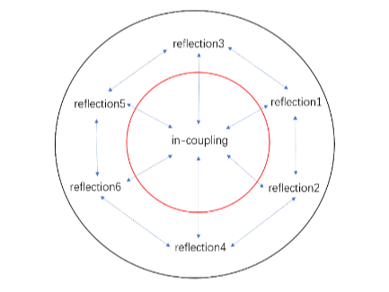
Figure 8: (c) Two-dimensional raster K-domain map.
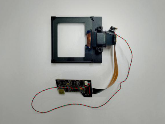
Figure 9: (a) Longjing Optoelectronics ’first generation grating waveguide sample diagram;
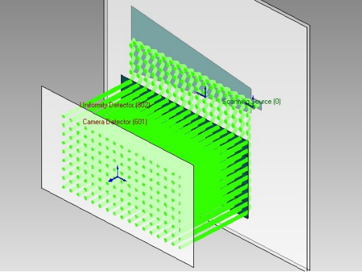
Figure 9: (b) Longjing photoelectric one-dimensional diffractive waveguide field tracking diagram;
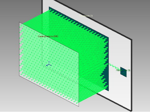
Figure 9: (c) Longjing Optoelectronics II -Dimensional diffractive waveguide field tracing diagram
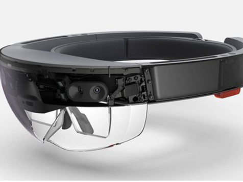
Figure 10: (a) rendering of Microsoft Hololens2;
Figure 10: (b) Waveoptics diffraction waveguide renderings;
Figure 10: (c) Dispelix diffraction waveguide renderings.
4. Volume holographic waveguide solution
Volume holographic grating waveguide scheme uses volume holographic grating as the coupling-in and coupling-out device of the waveguide. Volume holographic grating is an optical element with a periodic structure. It is generally exposed to the thickness of micron level through the double-beam holographic exposure method. Interference in the photopolymer film causes periodic changes in its refractive index, resulting in a nanoscale grating structure that can diffract incident light. Combining the volume holographic grating and the waveguide plate, the diffraction efficiency of the volume holographic grating can be adjusted by designing the relevant parameters of the volume holographic grating (such as material refractive index n, refractive index modulation factor and thickness, etc.). Currently, the representative manufacturers using volume holographic grating waveguide solutions are Sony and Digilens. Sony has only produced a single green volume holographic grating waveguide. The product is shown in Fig. 11 (a) [7], which has been discontinued. Digilens currently has double-layer full-color volume holographic grating waveguides, and the products are shown in Figure 11 (b) [8]. Fig. 11 (c) is a simulation verification of the optical path of our Longjing photoelectric holographic grating waveguide. Fig. 11 (d) is a sample of a single-layer full-color holographic grating waveguide developed by Longjing Optoelectronics. The field of view angle is 20 °. The corresponding display effect.

Figure 11: (a) Sony holographic grating Waveguide renderings;
Figure 11: (b) The renderings of Digilens holographic grating waveguide products;
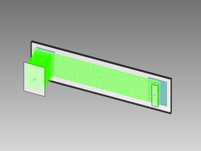
Figure 11: (c) Longjing photoelectric holographic grating waveguide field tracking diagram;
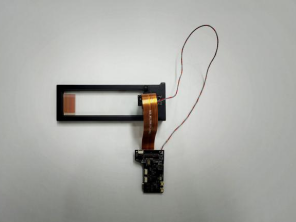
Figure 11: (d) Longjing photoelectric single-layer full-color holographic grating waveguide sample map.
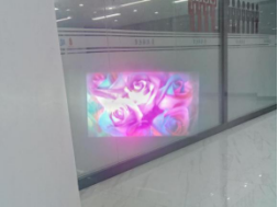
Figure 12: Actual effect of Longjing photoelectric single-layer full-color holographic grating waveguide
5. Off-axis holographic lens solution
Holographic laser retina projection uses a combination of MEMS laser scanning projection device and off-axis holographic lens to redirect the light incident on the holographic optical element to the human eye to realize the display of virtual images. MEMS laser scanning technology realizes scanning imaging by changing the orientation of the galvanometer mirror so that the incident beam exits in different directions. The off-axis holographic lens converts the divergent light of the MEMS scanning light source into convergent light into the human eye. The representative manufacturer currently adopting the holographic lens scheme is North. Figure 13 (a) is their sample picture [9], and the field angle is only 15 °. Figure 13 (b) is the optical path simulation of the off-axis holographic lens made by Longjing Optoelectronics. Figure 13 (c) is the sample of the long-term monochromatic off-axis holographic lens developed by Longjing Optoelectronics. Corresponding display effect, because MEMS is an ordinary projector that is temporarily purchased, the volume is large and the angle of view does not match, and the display effect can be significantly improved and the volume can be significantly reduced by customizing the MEMS projection device later.
Figure 13: (a) North holographic lens product renderings;
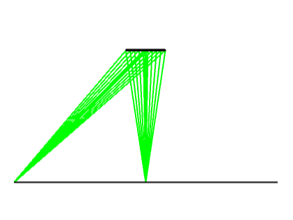
Figure 13: (b) Longjing photoelectric off-axis holographic optical path simulation diagram;
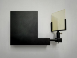
Figure 13: (c) Longjing photoelectric monochromatic off-axis holographic lens sample diagram;
Figure 13: (d) Longjing Photoelectric Single The actual rendering of chromatic off-axis holographic lens.
6. Micro-nano manufacturing of diffractive optical waveguides
6.1 Manufacturing of relief grating waveguide
As mentioned above, surface relief gratings can be divided into one-dimensional and two-dimensional gratings in dimension, and can be divided into straight grating, blazed grating and inclined grating in structure. Because the augmented reality optical waveguide is used in the visible light band, in order to achieve greater diffraction efficiency and field angle, its characteristic size is generally in the hundreds of nanometers, even tens of nanometers, and its performance is less tolerant to errors, so it Processing and preparation poses great challenges. At present, the preparation of diffractive optical waveguides is basically based on semiconductor manufacturing processes (such as photolithography and etching processes). However, because these methods are limited by their complicated and expensive equipment, the production cost is very high, which is not suitable for the mass production of optical modules.
Figure 14 shows the flow chart of the surface relief light grating template preparation or small batch preparation process, including its scanning electron microscope image. For straight gratings,The process is relatively mature. First, a resist layer is spin-coated on the substrate, the grating is patterned by interference exposure or electron beam exposure, and then the pattern is patterned by reactive ion etching (RIE) or inductively coupled plasma etching (ICP) Transfer to the substrate and remove the resist layer to complete the preparation of the straight grating. However, due to the uniformity problem, the inclined grating optical waveguide represented by HoloLens cannot be directly prepared by the reactive etching scheme, so the preparation process is more complicated, and focused ion beam etching (FIBE) and ion beam etching are required ( Ion beam etching (IBE), reactive ion beam etching (reactive ion beam etching, RIBE) technology. Considering the efficiency and uniformity comprehensively, RIBE is a more suitable solution. First, a hard mask (such as Cr) layer is physically or chemically coated on the substrate, and then a resist layer is spin-coated. The interference pattern or electron beam exposure is also used for patterning, and then the resist pattern is transferred to the Cr layer through a chlorine dry etching process. After the etching process, the remaining resist layer is stripped by the oxygen plasma method. Next, an ionized argon ion beam is used to enter the substrate at an oblique angle using a fluorine-based RIBE process. After reactive ion beam etching, the Cr mask is removed by a standard wet etching process to obtain an oblique grating with excellent uniformity.
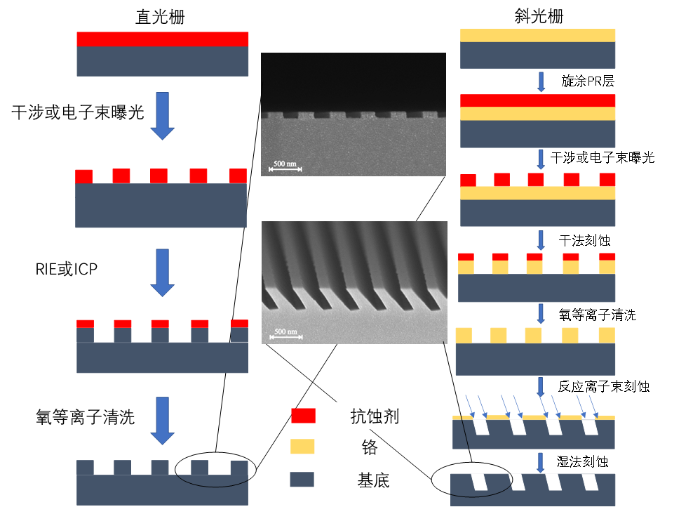
Figure 14: Surface relief grating template or small batch preparation process
The manufacturing cost based on the above-mentioned semiconductor technology is expensive, and it is not suitable for mass production processing of grating waveguides. Therefore, the replication process of diffractive optical waveguides was developed in order to achieve mass production, and this large-scale manufacturing process relies on high-refractive index optical resins. Currently, Magic Leap and WaveOptics have undergone related process verification. The replication process includes hot embossing, UV-nano imprint lithography, and micro contact printing (also known as soft lithography). Among them, ultraviolet nanoimprint lithography is a common method in mass production of surface relief grating waveguides.
The specific process flow is as followsAs shown in Figure 15, the process can be divided into two stages: the nano-imprint working mold preparation stage and the mass production stage. First, the pattern is processed onto a silicon wafer through the above template preparation process to be used as a template, and nano-imprint technology is used to spin-coat UV resin on a larger silicon wafer and print more templates on it. The printed structure is then exposed to ultraviolet light to fix the resin. Finally, by repeating the above process, a multi-pattern imprint mold is produced in batches. In the process of mass production, multi-patterned molds are used to produce surface-relief grating waveguides, then functional coatings are used to cover the waveguides, and laser cutting techniques are used to separate them. Finally, waveguides with different structures are stacked to realize the preparation of optical modules.
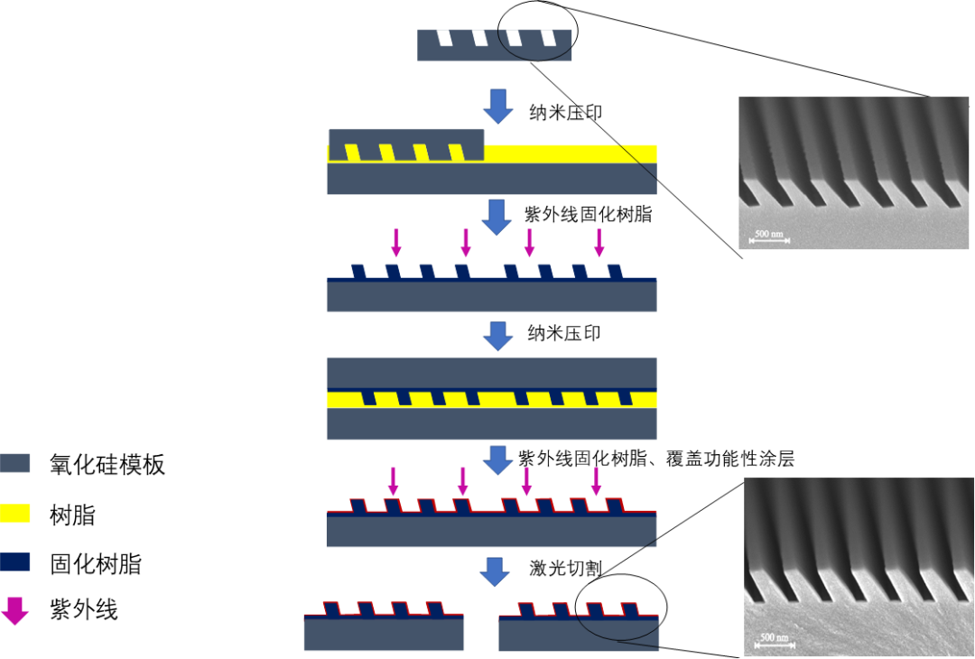
Figure 15: Mass production process of surface relief grating mass production
6.2 Volume holographic waveguide manufacturing
The basis for the preparation of volume holographic waveguides is interference exposure. By using a laser-excited interference pattern to expose the photosensitive refractive material attached to the substrate, the material properties change according to the intensity distribution of the light, and finally the one with periodic refractive index changes material. Materials for preparing volume holographic waveguides include silver halide, dichromate gelatin, photosensitive polymers, holographic polymer dispersed liquid crystal, and other more exotic materials. The recording process for volume holograms is mostly similar, but the general exposure is only suitable for small batch verification, and for mass production, it is necessary to develop more economical solutions. The companies represented by Sony and DigiLens have developed processing methods for volume holographic waveguides Process.
Figure 16 shows the roll-to-roll process for preparing volume holographic waveguides. First, the dual-beam interference exposure method is used to form a volume holographic waveguide in the photosensitive polymer film attached to the roll; second, the high-quality cycloolefin polymer plastic waveguide is formed by injection molding. In order to obtain a qualified image, the warpage of the waveguide must be less than 5um, and the thickness variation of the effective area should be less than 1um. Then, the holographic optical element transfer process is performed to accurately align and paste the holographic waveguide film with the plastic waveguide; then the plastic holographic waveguide is cut; finally, in the color matching process, the red and blue plastic waveguides are aligned with the green plastic waveguide and UV is used The resin fixes it. The plastic substrate should be kept flat before and after each processing. Both during stamping and color matchingThe challenge. Figure 16 shows photographs of green, red, blue, and full-color plastic VHG waveguides.
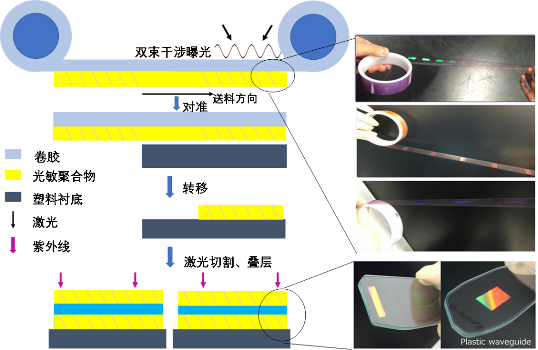
Figure 16: Roll-to-roll volume holographic waveguide preparation process
7. Outlook
The waveguide scheme in AR technology has gradually become the mainstream technology, so this article gives a detailed introduction to the geometric waveguide scheme (including the sawtooth waveguide scheme and the coated array waveguide scheme), the relief grating waveguide scheme, and the holographic grating waveguide scheme, and also introduces The holographic lens scheme, and showed some related samples of Longjing Optoelectronics. The prism scheme, the Birdbath scheme and the freeform scheme are not described in detail in this article due to the limitation of volume.
Polarized array waveguide solution has the advantages of light and thin, large eye movement range and good color uniformity. It has high technical barriers in design and processing. Long Jing Optoelectronics has been cultivating in this field for many years and has completely realized from design to processing The autonomy of the system has achieved mass production of coated array waveguides in China. Mature design solutions and large-scale mass production capabilities make polarization array waveguide solutions the mainstream solutions in the AR field in the next five years.
The sawtooth waveguide scheme has the same processing route and the same process difficulty as the polarization array waveguide scheme, but the sawtooth waveguide has serious stray light, low energy utilization, low contrast, and general imaging resolution, so sawtooth waveguide It is difficult for the solution to become the mainstream solution in the AR field.
The relief grating waveguide solution has the advantages of a large field of view and a large eye movement range. At the same time, due to the convenience of nano-imprinting, it has received more and more attention . However, the current main problems of the relief grating waveguide are: 1. color unevenness and rainbow effect; 2. the image information is coupled out on both sides of the waveguide sheet caused by the reflection and transmission order characteristics; 3. the good of nano-imprint Rate problem. Therefore, it is difficult for the relief grating waveguide solution to become the mainstream solution in a short time. The designIt is expected that the further maturity of the scheme and the improvement of the mass production yield will take some time. Longjing Optoelectronics and Hunan University are actively carrying out industry-university-research cooperation on relief grating waveguides, and jointly established the Micro-Nano Optical Research Center of Longjing Optoelectronics-Hunan University Shenzhen Research Institute, actively deploying micro-nano processing equipment to promote relief grating waveguides in design and processing Program development.
The volume holographic grating waveguide solution has the advantages of good color uniformity and easy realization of a monolithic color waveguide, but its use of holographic interference exposure for waveguide processing limits its large-scale mass production. At the same time, the multi-layer holographic grating needs to be superimposed to enlarge the FOV, which increases the process difficulty, and the high-density exposure material is required to make the color waveguide sheet, which further increases the process difficulty. Therefore, the volume holographic grating waveguide scheme is also difficult to become the mainstream scheme in a short time.
The holographic lens scheme uses the same holographic grating exposure process as the holographic grating waveguide scheme for processing, which has the advantage of a large FOV, but is limited by the effect of the eye movement range is too small, and is only used in individual fields. < / strong>.
In summary, The polarization array waveguide solution and the relief grating waveguide solution are currently the two most promising mainstream AR solutions, one representing the present and one representing the future . Long Jing Optoelectronics took the lead in realizing large-scale mass production of polarization array waveguides in China, and actively deployed relief grating waveguide solutions.
Reference content:
[1]. Wenjun Zhang, Zhifeng Wang, and Jian Xu, “Research on a surface-relief optical waveguide augmented reality display device,” Appl. Opt. 57, 3720-3729 (2018)
[2]. Miaomiao Xu, Hong Hua, “Ultrathin optical combiner with microstructure mirrors in augmented reality,” Proc. SPIE 10676, Digital Optics for Immersive Displays, 1067614 (21 May 2018); https://doi.org /10.1117/12.231562
[3]. https://lumusvision.com/products/oe33/
[4]. https://www.microsoft.com/zh-cn/hololens/hardware
[5]. https://enhancedworld.com/
[6]. https://www.dispelix.com/
[7]. https://image.baidu.com
[8]. www.digilens.com
[9]. www.bynorth.com
The relief grating waveguide scheme is to use the relief grating (SRG) instead of the traditional catadioptric optical device (ROE) as the coupling scheme in the waveguide scheme, coupling out and out pupil expansion device. Commonly used relief gratings mainly include one-dimensional gratings, including inclined gratings, trapezoidal gratings, blazed gratings and rectangular grating structures. Figure 7 (a) shows the scanning electron microscope (SEM) images of inclined gratings. A two-dimensional grating, such as a hexagonal cylindrical grating structure commonly used in waveguides, Figure 7 (b) shows an SEM image of the two-dimensional cylindrical grating structure. The feature sizes of the above grating structures are all on the nanometer scale.
So the current route of the relief grating waveguide mainly includes: a relief grating waveguide scheme based on a one-dimensional grating. The schematic diagram is shown in Figure 8 (a), which is divided into coupling, turning, and coupling out regions. The one-dimensional grating is expanded in one direction at the turning area and the decoupling area, respectively, and the representative product is HoloLens. Relief grating waveguide scheme based on two-dimensional grating,The schematic diagram is shown in Figure 8 (b), which is divided into coupling-in and coupling-out regions. The classical structure of the coupling-in region is a one-dimensional grating, and the structure of the coupling-out region is a two-dimensional grating, using multiple levels of the two-dimensional grating structure. At the same time to ensure the coupling of the beam and the expansion of multiple directions, the representative company is WaveOptics. Fig. 8 (c) is the K-domain diagram of the two-dimensional grating waveguide. The inner circle represents the total reflection condition in the waveguide plate, and the outer circle represents the maximum K value that can be achieved by the material of the waveguide plate. The coupled K grating translates the K value of the beam to The ring-shaped area, that is, the beam meets the conditions for total reflection propagation in the waveguide plate, the coupling-out grating translates the K value of part of the beam from the ring-shaped area to the inner-circle area, that is, the beam is coupled out to the human eye.
Figure 9 (a) shows the first generation of relief grating waveguide designed by Long Jing Optoelectronics. The two-dimensional grating waveguide solution used by Long Jing Optoelectronics. The relief grating waveguide with independent intellectual property rights of Long Jing Optoelectronics is also being developed and perfected. As shown in Fig. 9 (b) and Fig. 9 (c), they are the field tracking simulation results based on the two relief grating waveguide principles made by our company.
Figure 10 (a) is the effect picture of Microsoft’s latest Hololens2 [4], Figure 10 (b) is the effect picture of WaveOpics diffraction waveguide [5], and Figure 10 (c) is the effect picture of Dispelix diffraction waveguide [6] ]. These three companies are currently representative companies in relief relief waveguides abroad.
The relief grating waveguide uses the photolithography process to process the wafer as a master, and uses the nano-imprint process for large-scale replication and mass production. See below for details.
Figure 7: (a) inclined grating structure diagram;
Figure 7: (b) 2D cylindrical grating Structural drawing.
Figure 8: (a) Schematic diagram of one-dimensional grating waveguide;
Figure 8: (b) Schematic diagram of two-dimensional grating waveguide;
Figure 8: (c) Two-dimensional raster K-domain map.
Figure 9: (a) Longjing Optoelectronics ’first generation grating waveguide sample diagram;
Figure 9: (b) Longjing photoelectric one-dimensional diffractive waveguide field tracking diagram;
Figure 9: (c) Longjing Optoelectronics II -Dimensional diffractive waveguide field tracing diagram
Figure 10: (a) rendering of Microsoft Hololens2;
Figure 10: (b) Waveoptics diffraction waveguide renderings;
Figure 10: (c) Dispelix diffraction waveguide renderings.
4. Volume holographic waveguide solution
Volume holographic grating waveguide scheme uses volume holographic grating as the coupling-in and coupling-out device of the waveguide. Volume holographic grating is an optical element with a periodic structure. It is generally exposed to the thickness of micron level through the double-beam holographic exposure method. Interference in the photopolymer film causes periodic changes in its refractive index, resulting in a nanoscale grating structure that can diffract incident light. Combining the volume holographic grating and the waveguide plate, the diffraction efficiency of the volume holographic grating can be adjusted by designing the relevant parameters of the volume holographic grating (such as material refractive index n, refractive index modulation factor and thickness, etc.). Currently, the representative manufacturers using volume holographic grating waveguide solutions are Sony and Digilens. Sony has only produced a single green volume holographic grating waveguide. The product is shown in Fig. 11 (a) [7], which has been discontinued. Digilens currently has double-layer full-color volume holographic grating waveguides, and the products are shown in Figure 11 (b) [8]. Fig. 11 (c) is a simulation verification of the optical path of our Longjing photoelectric holographic grating waveguide. Fig. 11 (d) is a sample of a single-layer full-color holographic grating waveguide developed by Longjing Optoelectronics. The field of view angle is 20 °. The corresponding display effect.
Figure 11: (a) Sony holographic grating Waveguide renderings;
Figure 11: (b) The renderings of Digilens holographic grating waveguide products;
Figure 11: (c) Longjing photoelectric holographic grating waveguide field tracking diagram;
Figure 11: (d) Longjing photoelectric single-layer full-color holographic grating waveguide sample map.
Figure 12: Actual effect of Longjing photoelectric single-layer full-color holographic grating waveguide
5. Off-axis holographic lens solution
Holographic laser retina projection uses a combination of MEMS laser scanning projection device and off-axis holographic lens to redirect the light incident on the holographic optical element to the human eye to realize the display of virtual images. MEMS laser scanning technology realizes scanning imaging by changing the orientation of the galvanometer mirror so that the incident beam exits in different directions. The off-axis holographic lens converts the divergent light of the MEMS scanning light source into convergent light into the human eye. The representative manufacturer currently adopting the holographic lens scheme is North. Figure 13 (a) is their sample picture [9], and the field angle is only 15 °. Figure 13 (b) is the optical path simulation of the off-axis holographic lens made by Longjing Optoelectronics. Figure 13 (c) is the sample of the long-term monochromatic off-axis holographic lens developed by Longjing Optoelectronics. Corresponding display effect, because MEMS is an ordinary projector that is temporarily purchased, the volume is large and the angle of view does not match, and the display effect can be significantly improved and the volume can be significantly reduced by customizing the MEMS projection device later.
Figure 13: (a) North holographic lens product renderings;
Figure 13: (b) Longjing photoelectric off-axis holographic optical path simulation diagram;
Figure 13: (c) Longjing photoelectric monochromatic off-axis holographic lens sample diagram;
Figure 13: (d) Longjing Photoelectric Single The actual rendering of chromatic off-axis holographic lens.
6. Micro-nano manufacturing of diffractive optical waveguides
6.1 Manufacturing of relief grating waveguide
As mentioned above, surface relief gratings can be divided into one-dimensional and two-dimensional gratings in dimension, and can be divided into straight grating, blazed grating and inclined grating in structure. Because the augmented reality optical waveguide is used in the visible light band, in order to achieve greater diffraction efficiency and field angle, its characteristic size is generally in the hundreds of nanometers, even tens of nanometers, and its performance is less tolerant to errors, so it Processing and preparation poses great challenges. At present, the preparation of diffractive optical waveguides is basically based on semiconductor manufacturing processes (such as photolithography and etching processes). However, because these methods are limited by their complicated and expensive equipment, the production cost is very high, which is not suitable for the mass production of optical modules.
Figure 14 shows the flow chart of the surface relief light grating template preparation or small batch preparation process, including its scanning electron microscope image. For straight gratings,The process is relatively mature. First, a resist layer is spin-coated on the substrate, the grating is patterned by interference exposure or electron beam exposure, and then the pattern is patterned by reactive ion etching (RIE) or inductively coupled plasma etching (ICP) Transfer to the substrate and remove the resist layer to complete the preparation of the straight grating. However, due to the uniformity problem, the inclined grating optical waveguide represented by HoloLens cannot be directly prepared by the reactive etching scheme, so the preparation process is more complicated, and focused ion beam etching (FIBE) and ion beam etching are required ( Ion beam etching (IBE), reactive ion beam etching (reactive ion beam etching, RIBE) technology. Considering the efficiency and uniformity comprehensively, RIBE is a more suitable solution. First, a hard mask (such as Cr) layer is physically or chemically coated on the substrate, and then a resist layer is spin-coated. The interference pattern or electron beam exposure is also used for patterning, and then the resist pattern is transferred to the Cr layer through a chlorine dry etching process. After the etching process, the remaining resist layer is stripped by the oxygen plasma method. Next, an ionized argon ion beam is used to enter the substrate at an oblique angle using a fluorine-based RIBE process. After reactive ion beam etching, the Cr mask is removed by a standard wet etching process to obtain an oblique grating with excellent uniformity.
Figure 14: Surface relief grating template or small batch preparation process
The manufacturing cost based on the above-mentioned semiconductor technology is expensive, and it is not suitable for mass production processing of grating waveguides. Therefore, the replication process of diffractive optical waveguides was developed in order to achieve mass production, and this large-scale manufacturing process relies on high-refractive index optical resins. Currently, Magic Leap and WaveOptics have undergone related process verification. The replication process includes hot embossing, UV-nano imprint lithography, and micro contact printing (also known as soft lithography). Among them, ultraviolet nanoimprint lithography is a common method in mass production of surface relief grating waveguides.
The specific process flow is as followsAs shown in Figure 15, the process can be divided into two stages: the nano-imprint working mold preparation stage and the mass production stage. First, the pattern is processed onto a silicon wafer through the above template preparation process to be used as a template, and nano-imprint technology is used to spin-coat UV resin on a larger silicon wafer and print more templates on it. The printed structure is then exposed to ultraviolet light to fix the resin. Finally, by repeating the above process, a multi-pattern imprint mold is produced in batches. In the process of mass production, multi-patterned molds are used to produce surface-relief grating waveguides, then functional coatings are used to cover the waveguides, and laser cutting techniques are used to separate them. Finally, waveguides with different structures are stacked to realize the preparation of optical modules.
Figure 15: Mass production process of surface relief grating mass production
6.2 Volume holographic waveguide manufacturing
The basis for the preparation of volume holographic waveguides is interference exposure. By using a laser-excited interference pattern to expose the photosensitive refractive material attached to the substrate, the material properties change according to the intensity distribution of the light, and finally the one with periodic refractive index changes material. Materials for preparing volume holographic waveguides include silver halide, dichromate gelatin, photosensitive polymers, holographic polymer dispersed liquid crystal, and other more exotic materials. The recording process for volume holograms is mostly similar, but the general exposure is only suitable for small batch verification, and for mass production, it is necessary to develop more economical solutions. The companies represented by Sony and DigiLens have developed processing methods for volume holographic waveguides Process.
Figure 16 shows the roll-to-roll process for preparing volume holographic waveguides. First, the dual-beam interference exposure method is used to form a volume holographic waveguide in the photosensitive polymer film attached to the roll; second, the high-quality cycloolefin polymer plastic waveguide is formed by injection molding. In order to obtain a qualified image, the warpage of the waveguide must be less than 5um, and the thickness variation of the effective area should be less than 1um. Then, the holographic optical element transfer process is performed to accurately align and paste the holographic waveguide film with the plastic waveguide; then the plastic holographic waveguide is cut; finally, in the color matching process, the red and blue plastic waveguides are aligned with the green plastic waveguide and UV is used The resin fixes it. The plastic substrate should be kept flat before and after each processing. Both during stamping and color matchingThe challenge. Figure 16 shows photographs of green, red, blue, and full-color plastic VHG waveguides.
Figure 16: Roll-to-roll volume holographic waveguide preparation process
7. Outlook
The waveguide scheme in AR technology has gradually become the mainstream technology, so this article gives a detailed introduction to the geometric waveguide scheme (including the sawtooth waveguide scheme and the coated array waveguide scheme), the relief grating waveguide scheme, and the holographic grating waveguide scheme, and also introduces The holographic lens scheme, and showed some related samples of Longjing Optoelectronics. The prism scheme, the Birdbath scheme and the freeform scheme are not described in detail in this article due to the limitation of volume.
Polarized array waveguide solution has the advantages of light and thin, large eye movement range and good color uniformity. It has high technical barriers in design and processing. Long Jing Optoelectronics has been cultivating in this field for many years and has completely realized from design to processing The autonomy of the system has achieved mass production of coated array waveguides in China. Mature design solutions and large-scale mass production capabilities make polarization array waveguide solutions the mainstream solutions in the AR field in the next five years.
The sawtooth waveguide scheme has the same processing route and the same process difficulty as the polarization array waveguide scheme, but the sawtooth waveguide has serious stray light, low energy utilization, low contrast, and general imaging resolution, so sawtooth waveguide It is difficult for the solution to become the mainstream solution in the AR field.
The relief grating waveguide solution has the advantages of a large field of view and a large eye movement range. At the same time, due to the convenience of nano-imprinting, it has received more and more attention . However, the current main problems of the relief grating waveguide are: 1. color unevenness and rainbow effect; 2. the image information is coupled out on both sides of the waveguide sheet caused by the reflection and transmission order characteristics; 3. the good of nano-imprint Rate problem. Therefore, it is difficult for the relief grating waveguide solution to become the mainstream solution in a short time. The designIt is expected that the further maturity of the scheme and the improvement of the mass production yield will take some time. Longjing Optoelectronics and Hunan University are actively carrying out industry-university-research cooperation on relief grating waveguides, and jointly established the Micro-Nano Optical Research Center of Longjing Optoelectronics-Hunan University Shenzhen Research Institute, actively deploying micro-nano processing equipment to promote relief grating waveguides in design and processing Program development.
The volume holographic grating waveguide solution has the advantages of good color uniformity and easy realization of a monolithic color waveguide, but its use of holographic interference exposure for waveguide processing limits its large-scale mass production. At the same time, the multi-layer holographic grating needs to be superimposed to enlarge the FOV, which increases the process difficulty, and the high-density exposure material is required to make the color waveguide sheet, which further increases the process difficulty. Therefore, the volume holographic grating waveguide scheme is also difficult to become the mainstream scheme in a short time.
The holographic lens scheme uses the same holographic grating exposure process as the holographic grating waveguide scheme for processing, which has the advantage of a large FOV, but is limited by the effect of the eye movement range is too small, and is only used in individual fields. < / strong>.
In summary, The polarization array waveguide solution and the relief grating waveguide solution are currently the two most promising mainstream AR solutions, one representing the present and one representing the future . Long Jing Optoelectronics took the lead in realizing large-scale mass production of polarization array waveguides in China, and actively deployed relief grating waveguide solutions.
Reference content:
[1]. Wenjun Zhang, Zhifeng Wang, and Jian Xu, “Research on a surface-relief optical waveguide augmented reality display device,” Appl. Opt. 57, 3720-3729 (2018)
[2]. Miaomiao Xu, Hong Hua, “Ultrathin optical combiner with microstructure mirrors in augmented reality,” Proc. SPIE 10676, Digital Optics for Immersive Displays, 1067614 (21 May 2018); https://doi.org /10.1117/12.231562
[3]. https://lumusvision.com/products/oe33/
[4]. https://www.microsoft.com/zh-cn/hololens/hardware
[5]. https://enhancedworld.com/
[6]. https://www.dispelix.com/
[7]. https://image.baidu.com
[8]. www.digilens.com
[9]. www.bynorth.com
Holographic laser retina projection uses a combination of MEMS laser scanning projection device and off-axis holographic lens to redirect the light incident on the holographic optical element to the human eye to realize the display of virtual images. MEMS laser scanning technology realizes scanning imaging by changing the orientation of the galvanometer mirror so that the incident beam exits in different directions. The off-axis holographic lens converts the divergent light of the MEMS scanning light source into convergent light into the human eye. The representative manufacturer currently adopting the holographic lens scheme is North. Figure 13 (a) is their sample picture [9], and the field angle is only 15 °. Figure 13 (b) is the optical path simulation of the off-axis holographic lens made by Longjing Optoelectronics. Figure 13 (c) is the sample of the long-term monochromatic off-axis holographic lens developed by Longjing Optoelectronics. Corresponding display effect, because MEMS is an ordinary projector that is temporarily purchased, the volume is large and the angle of view does not match, and the display effect can be significantly improved and the volume can be significantly reduced by customizing the MEMS projection device later.
Figure 13: (a) North holographic lens product renderings;
Figure 13: (b) Longjing photoelectric off-axis holographic optical path simulation diagram;
Figure 13: (c) Longjing photoelectric monochromatic off-axis holographic lens sample diagram;
Figure 13: (d) Longjing Photoelectric Single The actual rendering of chromatic off-axis holographic lens.
6. Micro-nano manufacturing of diffractive optical waveguides
6.1 Manufacturing of relief grating waveguide
As mentioned above, surface relief gratings can be divided into one-dimensional and two-dimensional gratings in dimension, and can be divided into straight grating, blazed grating and inclined grating in structure. Because the augmented reality optical waveguide is used in the visible light band, in order to achieve greater diffraction efficiency and field angle, its characteristic size is generally in the hundreds of nanometers, even tens of nanometers, and its performance is less tolerant to errors, so it Processing and preparation poses great challenges. At present, the preparation of diffractive optical waveguides is basically based on semiconductor manufacturing processes (such as photolithography and etching processes). However, because these methods are limited by their complicated and expensive equipment, the production cost is very high, which is not suitable for the mass production of optical modules.
Figure 14 shows the flow chart of the surface relief light grating template preparation or small batch preparation process, including its scanning electron microscope image. For straight gratings,The process is relatively mature. First, a resist layer is spin-coated on the substrate, the grating is patterned by interference exposure or electron beam exposure, and then the pattern is patterned by reactive ion etching (RIE) or inductively coupled plasma etching (ICP) Transfer to the substrate and remove the resist layer to complete the preparation of the straight grating. However, due to the uniformity problem, the inclined grating optical waveguide represented by HoloLens cannot be directly prepared by the reactive etching scheme, so the preparation process is more complicated, and focused ion beam etching (FIBE) and ion beam etching are required ( Ion beam etching (IBE), reactive ion beam etching (reactive ion beam etching, RIBE) technology. Considering the efficiency and uniformity comprehensively, RIBE is a more suitable solution. First, a hard mask (such as Cr) layer is physically or chemically coated on the substrate, and then a resist layer is spin-coated. The interference pattern or electron beam exposure is also used for patterning, and then the resist pattern is transferred to the Cr layer through a chlorine dry etching process. After the etching process, the remaining resist layer is stripped by the oxygen plasma method. Next, an ionized argon ion beam is used to enter the substrate at an oblique angle using a fluorine-based RIBE process. After reactive ion beam etching, the Cr mask is removed by a standard wet etching process to obtain an oblique grating with excellent uniformity.
Figure 14: Surface relief grating template or small batch preparation process
The manufacturing cost based on the above-mentioned semiconductor technology is expensive, and it is not suitable for mass production processing of grating waveguides. Therefore, the replication process of diffractive optical waveguides was developed in order to achieve mass production, and this large-scale manufacturing process relies on high-refractive index optical resins. Currently, Magic Leap and WaveOptics have undergone related process verification. The replication process includes hot embossing, UV-nano imprint lithography, and micro contact printing (also known as soft lithography). Among them, ultraviolet nanoimprint lithography is a common method in mass production of surface relief grating waveguides.
The specific process flow is as followsAs shown in Figure 15, the process can be divided into two stages: the nano-imprint working mold preparation stage and the mass production stage. First, the pattern is processed onto a silicon wafer through the above template preparation process to be used as a template, and nano-imprint technology is used to spin-coat UV resin on a larger silicon wafer and print more templates on it. The printed structure is then exposed to ultraviolet light to fix the resin. Finally, by repeating the above process, a multi-pattern imprint mold is produced in batches. In the process of mass production, multi-patterned molds are used to produce surface-relief grating waveguides, then functional coatings are used to cover the waveguides, and laser cutting techniques are used to separate them. Finally, waveguides with different structures are stacked to realize the preparation of optical modules.
Figure 15: Mass production process of surface relief grating mass production
6.2 Volume holographic waveguide manufacturing
The basis for the preparation of volume holographic waveguides is interference exposure. By using a laser-excited interference pattern to expose the photosensitive refractive material attached to the substrate, the material properties change according to the intensity distribution of the light, and finally the one with periodic refractive index changes material. Materials for preparing volume holographic waveguides include silver halide, dichromate gelatin, photosensitive polymers, holographic polymer dispersed liquid crystal, and other more exotic materials. The recording process for volume holograms is mostly similar, but the general exposure is only suitable for small batch verification, and for mass production, it is necessary to develop more economical solutions. The companies represented by Sony and DigiLens have developed processing methods for volume holographic waveguides Process.
Figure 16 shows the roll-to-roll process for preparing volume holographic waveguides. First, the dual-beam interference exposure method is used to form a volume holographic waveguide in the photosensitive polymer film attached to the roll; second, the high-quality cycloolefin polymer plastic waveguide is formed by injection molding. In order to obtain a qualified image, the warpage of the waveguide must be less than 5um, and the thickness variation of the effective area should be less than 1um. Then, the holographic optical element transfer process is performed to accurately align and paste the holographic waveguide film with the plastic waveguide; then the plastic holographic waveguide is cut; finally, in the color matching process, the red and blue plastic waveguides are aligned with the green plastic waveguide and UV is used The resin fixes it. The plastic substrate should be kept flat before and after each processing. Both during stamping and color matchingThe challenge. Figure 16 shows photographs of green, red, blue, and full-color plastic VHG waveguides.
Figure 16: Roll-to-roll volume holographic waveguide preparation process