For the first time, semiconductor carbon nanotubes surpass similar-sized silicon-based CMOS devices and circuits in real electronics performance.
On May 22, the Zhang Zhiyong-Peng Lianmao research group of the Carbon-based Electronics Research Center of the Department of Electronics, Peking University and the Key Laboratory of Nanodevice Physics and Chemistry of the Ministry of Education was in Published a paper in the top academic journal “Science”, entitled “Aligned, high-density semiconducting carbon nanotube arrays for high-performance electronics”.
The paper describes the preparation of high-density and high-purity semiconductor array carbon nanotube materials on a 4-inch substrate, breaking through the key material bottleneck of carbon nanotube integrated circuits. Zhang Zhiyong told Peng Mei News At present, the research team can actually prepare such carbon tubes on 8-inch wafers, and has developed fully automated purification and assembly equipment, fully equipped with mass production technology accumulation.
Requirements for large-scale integrated circuits on carbon tube materials
New materials to combat the “short channel effect”
Requirements for large-scale integrated circuits on carbon tube materials
New materials to combat the “short channel effect”
Transistors whose size is comparable to cells are the basic “bricks” for building chips. Currently, the most mainstream logic circuits designed in the electronics industry are complementary metal oxide semiconductor (CMOS) technologies, which are composed of P-type and N-type MOS transistors. Among them, a thin layer of semiconductor called “channel” connecting the source and drain regions is very important.
According to the famous description of “Moore’s Law”, when the price is unchanged, the number of components that can be accommodated on the integrated circuit will increase approximately every 18-24 months Doubled, performance has doubled. Once the CMOS transistor is reduced to the sub-10nm technology node, the channel length will be shortened accordingly, and the “short channel effect” will appear.Remove some device functions.
Therefore, scientists are exploring the use of new structures or new materials to solve this problem, and further improve the energy efficiency of the device.
Among many new semiconductor materials, semiconductor carbon nanotubes have attracted some attention: it has ultra-high electron and hole mobility, atomic-scale thickness, and The stable structure is an ideal channel material for building high-performance CMOS devices.
Zhang Zhiyong-Peng Lianmao ’s research group published an article in Science in 2017, which showed that according to the previous experimental results, the planar structure of carbon nanotube CMOS transistors can be reduced Up to 5nm gate length, and compared with the same gate length of silicon-based CMOS devices have 10 times the intrinsic performance power advantages.
However, to realize the potential of this experiment, the technical foundation for preparation, purification and arrangement of materials is also required.
Preparation, purification and arrangement
Preparation, purification and arrangement
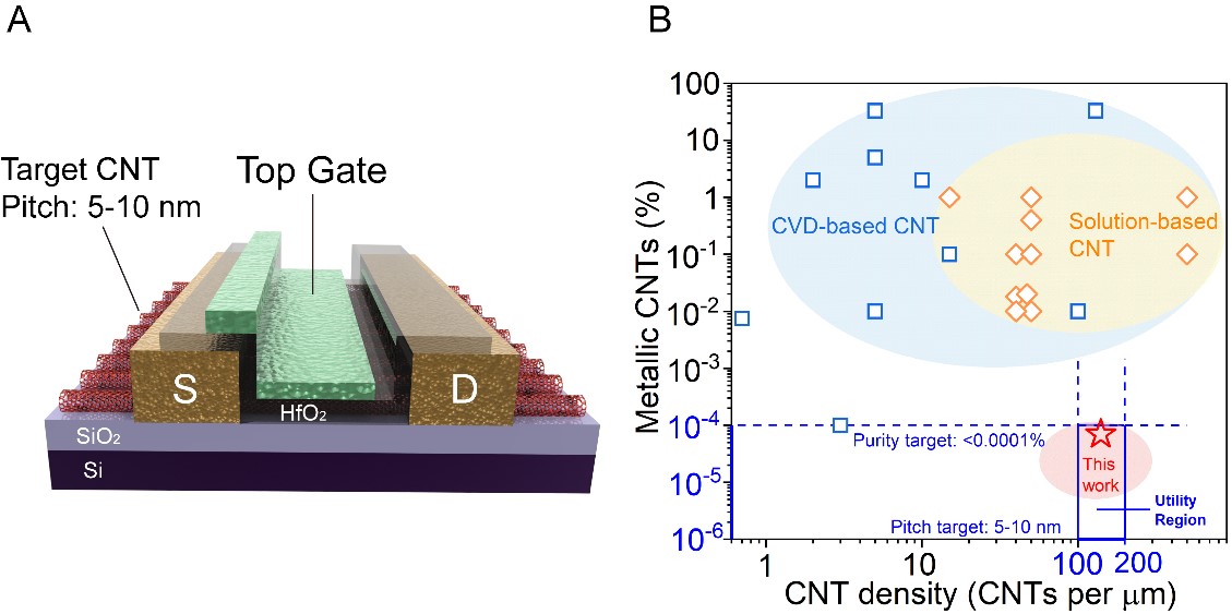
Carbon nanotube is a multi-layer circular tube composed of carbon atoms arranged in a hexagon. For a long time, the development of carbon nanotube integrated circuits has been restricted by material problems. The key is to achieve ultra-high semiconductor purity, alignment, high density, and uniformity over a large area.
The so-called ultra-high semiconductor purity and high density, the specific indicators are semiconductor purity exceeding 99.9999% and density reaching 100-200 per micron.
Although academia has developed a variety of methods for preparing, purifying, and arranging carbon nanotubes in the past 20 years, this goal has never been approached. This makes the actual performance of carbon nanotube transistors and circuits far below theoretical expectations, and even lags behind silicon-based technology of the same technology node by at least an order of magnitude.
For the preparation and purification, Zhang Zhiyong-Peng Lianmao research group used multiple-dispersion sorting process technology in the paper to obtain ultra-high purity Carbon nanotube solution.

Preparation and characterization of high-density and high-purity semiconductor carbon nanotube array
Preparation and characterization of high-density and high-purity semiconductor carbon nanotube array
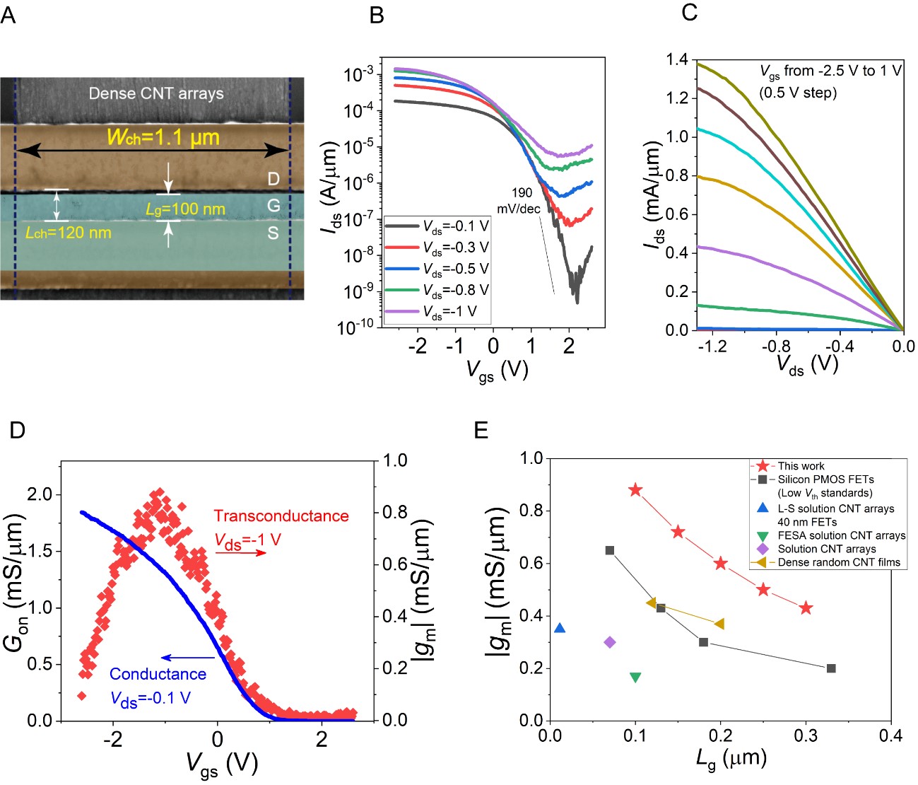
Next, in terms of alignment, the research team proposed a Dimension-Limited Self-Alignment method to prepare a density of 120 / micron on a 4-inch wafer, a semiconductor purity of up to 99.99995%, and a diameter distribution of 1.45 ± 0.23nm The array of carbon nanotubes theoretically meets the needs of ultra-large-scale carbon nanotube integrated circuits.
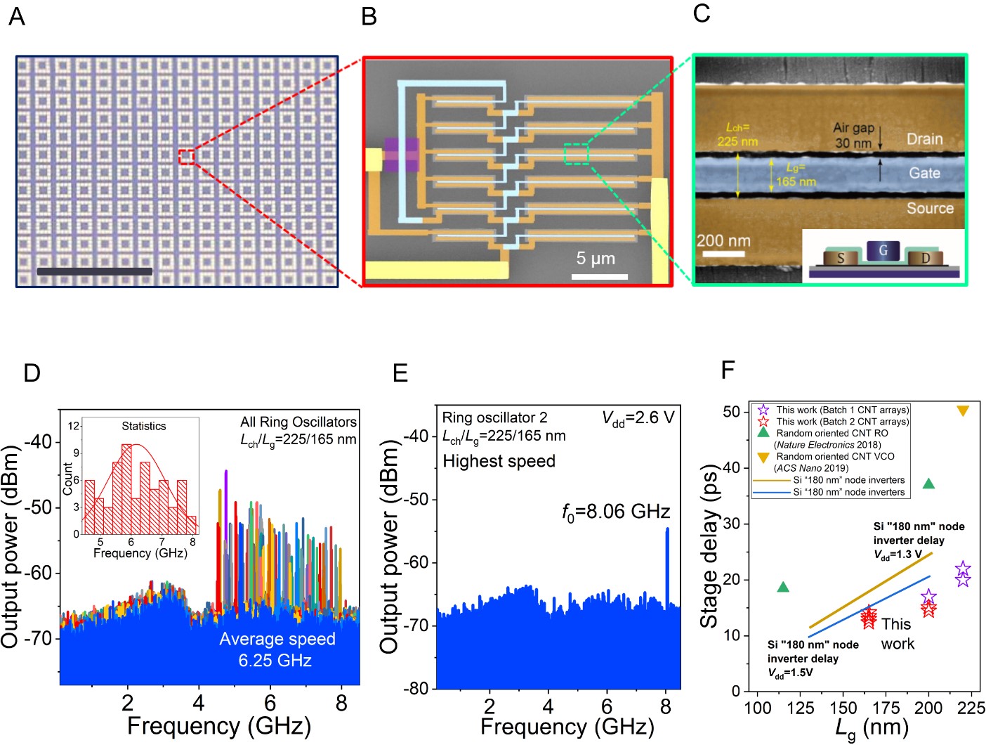
Based on this material, the research team prepared field effect transistors and ring oscillator circuits in batches. The transconductance and saturation current of carbon-based transistors with a 100-nanometer gate length reached 0.9, respectively mS / μm and 1.3mA / μm, the sub-threshold swing at room temperature is 90mV / dec; a fifth-order ring oscillator circuit is prepared in batches, the yield rate exceeds 50%, and the maximum oscillation frequency reaches 8.06GHz, far exceeding the published Circuits based on nanomaterials, and for the first time surpassed similar size silicon-based CMOS devices and circuits.
High-performance carbon nanotube transistor
The carbon-based integrated circuit has just started
High-performance carbon nanotube transistor
The carbon-based integrated circuit has just started
The paper looks at the end of the paper and needs to be applied to larger sizes (such as 8-inch wafers) in the future. And need to be further purified.
Zhang Zhiyong revealed to Peng Mei News that the research team has actually achieved preparation on 8-inch wafers. This is a technology that can be mass-produced and is growing rapidly.
In terms of purityAt present, the semiconductor purity of carbon nanotubes has reached 99.9999%, but for the application of very large scale integrated circuits, it needs to be further improved by 2-3 orders of magnitude. “Further purification will increase process steps and reduce production, and how to characterize such high purity, there are challenges, need to use engineering methods to overcome these challenges.” He said.
High-performance carbon nanotube transistor
High-performance carbon nanotube transistor
Zhang Zhiyong believes that this achievement The experiment shows the performance advantages of carbon nanotube devices and integrated circuits compared to traditional technologies, and takes the first step to promote the practical development of carbon-based integrated circuits.
He said that when the processing technology is not too mature, the carbon-based chip can be used as a supplement to the silicon-based chip to enhance the function or performance of the silicon-based chip, or Used for some special occasions. Once the technology is mature, the carbon-based chip may develop a complete application field and play an important role in the mainstream computing field.
The first author of the paper is Liu Lijun, a doctoral student of the Department of Electronics, Peking University and the engineer Han Jie, Zhang Zhiyong and Peng Lianmao are co-corresponding authors of the article, Xiangtan University, Hunan Province Advanced Relevant researchers from the Sensing and Information Technology Innovation Research Institute, Zhejiang University, Peking University Nano Optics Frontier Science Center and other units also participated in the cooperation.
This research was funded by the National Key R & D Program “Nanotechnology” key special project, Beijing Science and Technology Commission, National Natural Science Foundation of China and other projects.