Thanks to innovative miniature optical sensors
Figure | MEMS
Editor’s note: This article comes from the WeChat public account “MEMS” (ID: MEMSensor), the author’s consulting, the original title “Integrated nano-optical mechanical sensors, making nanometer measurement “on-chip laboratory” within reach“, slightly reduced.
According to Myers Consulting, researchers at the Eindhoven University of Technology in the Netherlands have developed a micro-integrated optical sensor that can provide higher resolution, making ultra-compact optics Possibly, including lasers and detectors for the “lab-on-chip” platform. The research results have been published in Nature Communications.
“Optical readout sensors based on optomechanical systems are already common in the field of sensing, such as atomic force microscopes (AFM).” Eindhoven University of Technology developers said, “Atomic force microscopes will be a pair The micro-cantilever, which is very sensitive to weak forces, is fixed at one end and has a tiny needle tip at the other end, which is in light contact with the surface of the sample. Fluctuations in the direction of the surface of the sample. Then, the laser beam is focused on the back of the micro cantilever, and the sub-nano resolution image can be obtained by measuring the change of the laser beam reflected by the cantilever on the surface of interest.”

With its compact optical sensor, “On-chip Nanometering Lab” is at your fingertips
However, traditional laser-based solutions such as atomic force microscopes are often bulky, coupled with the requirement for low cost and high resolution, which has driven the development of alternative solutions.
Thanks to the development of nano-optical mechanical systems, compact optical sensors can now be used to measure nano-scale motion, force and mass. However, one of the limiting factors is the need for a tunable laser with a narrow linewidth, and the integration of such devices still has challenges.
To solve this problem, Tianran Liu, Andrea Fiore of the Institute of Photonic Integration at Eindhoven University of Technology and colleagues designed a new optomechanical device with a resolution of up to 45 femtometres (45 x 10⁻¹⁵m), the measurement time is only a fraction of a second. The developer added: “The key is that the device has an ultra-wide optical bandwidth of 80 nanometers, which eliminates the need for tunable lasers.”
Four Waveguides and Large Wavelength Range
In the design of the sensor structure, light from an input waveguide superimposes symmetric and antisymmetric supermodes, and after a beat length in a directional coupler, constructive interference occurs at the “cross” output port . The displacement of one suspended waveguide changes the propagation constant of the supermode, causing destructive interference, thereby increasing the transmission of the other waveguide. The author explains that the change in the relative transmission of the two output waveguides is the result of the vertical and horizontal evanescent coupling.
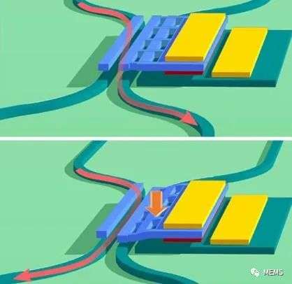
Drive the light passing through the directional coupler before (upper) and after (lower) the displacement of the suspended waveguide

In this study, the simulated electric field distribution of the ideal device before and after the suspension waveguide displacement (55 nm) (| E|)
This sensor is based on InP (membrane-on-silicon) platform and can be used for passive devices such as lasers or detectors. The sensor itself consists of four waveguides, two of which are suspended above the two output waveguides.
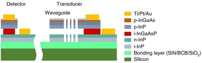
Sectional schematic of device stack
When the suspended waveguide is pushed to the output waveguide on the InP film, the relative signal amount on the output waveguide will change. Its manufacture uses a series of lithography steps to define the waveguide and cantilever. The final sensor consists of a sensor, actuator and photodiode.
An important advantage of this sensor is that it can work in a wide wavelength range, thus eliminating the requirement for expensive lasers on the device. In terms of deflection of the cantilever beam, the sensor also replicates the resolution of the cantilever beam of a traditional atomic force microscope. The researchers plan to build on this new device, build a tip on top of a movable waveguide, and develop a complete “nanometering laboratory” on an integrated chip for semiconductor metrology testing for next-generation microchips and nanometers Electronic design helps.