
Peng Lianmao, Professor of Peking University ’s Department of Electronics and Academician of Chinese Academy of Sciences. DeepTech Chart In 1947, Bell Labs demonstrated the world ’s first germanium semiconductor-based transistor, marking the beginning of the information age. In 1954, silicon transistors came out and subsequently became the mainstream of integrated circuit technology. More than 60 years later, “Moore’s Law” is dying. Will chip materials “change lanes” again?
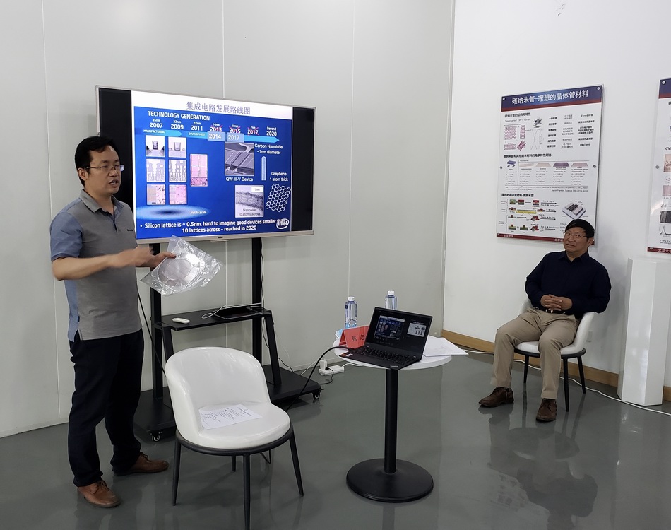
“We have been walking on the road of carbon-based integrated circuits for 20 years, and have not seen any obstacles that make us feel that we can’t go on.” Peking University School of Information Peng Lianmao, director of the Department of Electronics and an academician of the Chinese Academy of Sciences, said in an interview with Peng Mei News at the Beijing Carbon-based Integrated Circuit Research Institute. An 8-inch wafer in the hand is lined with carbon nanotube transistors.
Not long ago, the Zhang Zhiyong-Peng Lianmao research group just broke through the key material bottleneck of semiconductor carbon nanotubes, making the devices and circuits prepared by them behave in real electronics For the first time, it surpassed silicon-based products. Related results were published in the world’s top academic journal “Science” (Science).
Peng Lianmao believes that this is the first step for carbon-based integrated circuits to realize their theoretical potential. Although carbon-based nanomaterials were included in the International Semiconductor Technology Development Roadmap (ITRS) as a future technology option in 2009, the simulation results of IBM in the United States believe that planar structure carbon tube array transistors lead the silicon-based 5 technology nodes, but so far, semiconductor carbon Nanotube integrated circuits are considered to be comparable to the true performance of traditional technologies, far ahead of other non-silicon semiconductor materials, including the so-called third-generation semiconductors.
“At this point, we can start talking about industrialization of scale.” Peng Lianmao said. The team’s next goal is to complete the development of a 90-nanometer carbon-based CMOS pilot process within 2-3 years, with a performance equivalent to a 28-nanometer silicon-based device. Although it is not a high-end technology node, it is a threshold to enter the market.
Introducing the achievements of Zhang Zhiyong and Peng Lianmao. Integrated circuits involve a complex and long ecological chain, and the subsequent interconnection, packaging, and testing are not good at the Zhang Zhiyong-Peng Lianmao team. Link.
Changing from silicon to carbon, Zhang Zhiyong, a professor at Peking University ’s Institute of Physics and Electronics, said that if he wants to go through this new path, he has already done a good job. Preparation for many “pits”.
In fact, the breakthrough achieved this time belongs to the field of materials, and it is not the team ’s “old business”. “We are responsible Those who design and manufacture transistors with materials only wait for the materials for too long before they do it themselves. “Zhang Zhiyong said. Now with the materials they prepared, purified and arranged, they finally came to a” comfort zone “for 20 years, and it is expected that the next progress will be relatively smooth.
Breaking through Moore ’s Law
Transistors smaller than cells are the basic “bricks” for building chips, densely arranged on wafers .
At present, the most mainstream logic circuit designed by the electronics industry is complementary metal oxide semiconductor (CMOS) technology, which is composed of P-type and N-type MOS transistors. . Among them, a thin layer of semiconductor called “channel” connecting the source and drain regions is very important.
According to the famous “Moore’s Law”, when the price is unchanged, the number of components that can be accommodated on the integrated circuit will increase every 18-24 months Doubled, performance has doubled. This law accurately describes the development of human integrated circuit technology in the past few decades, but with the emergence of some bottleneck problems, since the 14 nm node, the actual progress has begun to be slower than Moore’s Law.
For example, a thin layer of semiconductor called a “channel” is very important for the source and drain regions of a CMOS transistor. Once the CMOS transistor is reduced to the sub-10nm technology node, the channel length will be shortened accordingly, and there will be a “short channel effect”, and some device functions will be lost.
When Moore’s Law “ends to life”, the industry has no final conclusion. But attempts to continue life for Moore’s Law include the use of new structures or new materials to solve short-channel effects and other issues to further improve device energy utilization.
Material bottleneck of carbon nanotubes
Peng Lianmao ’s early main direction was electron microscopy. Shortly after returning to Peking University in 2000, 38 At the age of four, he began to lead the research team to explore methods for preparing integrated circuits using carbon nanotube materials.
The so-called carbon nanotube is a new type of material discovered in 1991. It is a single-layer or multi-layer circular tube composed of hexagonal carbon atoms. In the preparation of high-performance transistors, it has the advantages of ultra-high electron and hole mobility, atomic thickness, and stable structure.
Peng Lianmao revealed that, in fact, in 1998, the IBM Watson Research Center and Delft University of Technology in the Netherlands had cooperated to make the world ’s first carbon Tube transistor. However, due to the constraints of material issues and the change in the company’s investment strategy, IBM later gave up this research.
Specifically, to achieve large-scale high-performance integrated circuits, carbon nanotubes must have ultra-high semiconductor purity, alignment, high density, and large area uniformity.
A commentary article published by Duke University professor Aaron Franklin in Nature in 2013 puts forward a quantitative indicator that the semiconductor purity exceeds 99.9999% (“6 9s”), the density reaches 100-200 per micron. Duke University is currently one of the main research positions in the world to tackle carbon nanotube integrated circuits.
Over the past 20 years, academia has developed a variety of methods for preparing, purifying, and arranging carbon nanotubes, but this practical area has never been accessible. This makes the actual performance of carbon nanotube transistors and circuits far below theoretical expectations, and even lags behind silicon-based technology of the same technology node by at least an order of magnitude.
20 years of exploring the road
In the first 7 years, the Peng Lianmao team “followed the car” along the international mainstream path After bumping, it finally formed a basic carbon tube preparation technology in 2007 and officially entered the field of carbon-based chips.
During the period of “following the car”, they never waited for a major breakthrough in the field of carbon tube materials, so in the next 10 years, the research group gave upIn the traditional doping process, a complete set of high-performance carbon nanotube transistor undoped preparation methods have been developed to break through the difficulty of preparing carbon-based N-type MOS tubes.
In 2017, the team first prepared a transistor with a gate length of 5 nanometers, which is the world ’s smallest high-performance transistor to date, and theoretically compared with the same size silicon-based transistor at that time It has a comprehensive advantage of 10 times the intrinsic performance and power consumption, and the results have appeared in the “Science” magazine for the first time.
So, how much of this theoretical advantage can be realized in the real performance of integrated circuits? This is the story told by the latest “Science” paper.
For the purity goal of “6 9s”, the research team used the technology of Multiple-Dispersion Sorting Process to obtain ultra-high purity carbon nanotubes Solution, semiconductor purity reaches 99.99995%.
Although this purification technology was first proposed by the US team, the research team has made many improvements in polymer selection, multiple purification processes and polymer separation .
Although it is an unfamiliar field, due to the relative shortage of domestic integrated circuit talents, materials and chemical experts are easy to find. With a team of about ten people, it surpassed internationally.
In terms of alignment, the research team proposes to combine the Dimension-Limited Self-Alignment method to prepare a density of 120 / micron on 4-inch wafers The carbon nanotube array with a diameter distribution of 1.45 ± 0.23nm theoretically meets the needs of ultra-large-scale carbon nanotube integrated circuits.
Based on this material, the researchers prepared field effect transistors and ring oscillator circuits in batches. The transconductance and saturation current of carbon-based transistors with a 100-nanometer gate length were 0.9 mS / μm and 1.3mA / μm, the sub-threshold swing at room temperature is 90mV / dec; a fifth-order ring oscillator circuit is prepared in batches, the yield exceeds 50%, and the maximum oscillation frequency reaches 8.06GHz, far exceeding the published Circuits based on nanomaterials, and for the first time surpassed similar size silicon-based CMOS devices and circuits.

The world ’s leading carbon chip technology. DeepTech map
The future of carbon-based chips
Zhang Zhiyong revealed that the progress made on carbon tube materials this time can at least maintain an international advantage for two years . “Now we feel that confidence has been greatly improved, and things that are not good can be done, and things that are good are sure to be okay.”
Testing on a 4-inch carbon-based integrated circuit At the site, technicians told Peng Mei reporters that carbon-based integrated circuit production is currently compatible with traditional silicon-based integrated circuit production equipment, and because of the characteristics of carbon nanotubes, the process flow is more concise.
Zhang Zhiyong said that the paper still reports the results on 4-inch wafers, and the research group can actually prepare on 8-inch wafers, “This is a kind of Technology that can be mass-produced and is developing rapidly. “
The team believes that in the process of developing a 90-nanometer carbon-based CMOS pilot process in the next 2-3 years, it faces Is more an engineering problem than a principle problem.
For example, in terms of purity, the current semiconductor purity of carbon nanotubes has reached six 9s, but for very large scale integrated circuit applications, it needs to be improved by 2 -3 orders of magnitude. “Further purification will increase process steps and reduce yield, and how to characterize such high purity, there are challenges, need to use engineering methods to overcome these challenges.” Zhang Zhiyong said.
In the farther future, if you want to realize the theoretical performance of the 5 nanometer gate length (corresponding to the silicon-based 1.5-2 nanometer technology node) carbon tube transistor in the laboratory, Many challenges are needed, such as chip design equipment and production process management.
Zhang Zhiyong believes that when the processing technology is not too mature, the carbon-based chip can be used as a supplement to the silicon-based chip to enhance the function or performance of the silicon-based chip, or Used for some special occasions. For example, carbon-based integrated circuits can realize new forms of chips such as flexibility and transparency, and have application prospects in special environments such as display, medical and health monitoring, radiation resistance, and near-infrared imaging.
But if it can be truly mature, carbon-based chips will be expected toTechnology advances to below 3 nanometer nodes, and its performance surpasses that of silicon-based chips by more than 10 times.